- 您現(xiàn)在的位置:買賣IC網(wǎng) > PDF目錄30737 > LC83026E SPECIALTY CONSUMER CIRCUIT, PQFP80 PDF資料下載
參數(shù)資料
| 型號(hào): | LC83026E |
| 元件分類: | 消費(fèi)家電 |
| 英文描述: | SPECIALTY CONSUMER CIRCUIT, PQFP80 |
| 封裝: | QFP-80 |
| 文件頁數(shù): | 12/16頁 |
| 文件大小: | 275K |
| 代理商: | LC83026E |
No. 5663-5/16
LC83026E
Continued from preceding page.
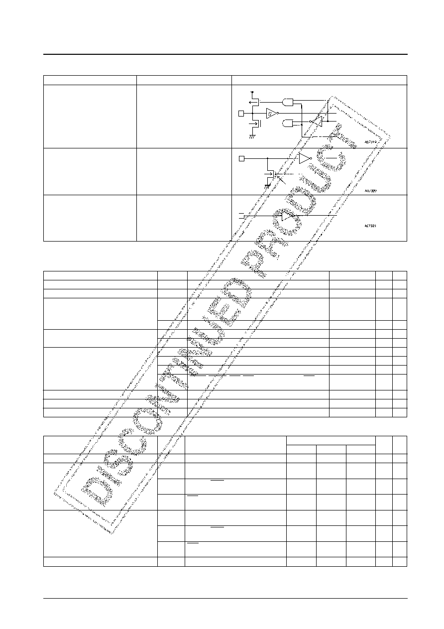
Pins
Specifications
Circuit
D0 to D7
CMOS intermediate current output
Low Schmitt input
P0 to P2
N-channel open drain intermediate
current output
Normal input
ADL1, ADR1, ADM1
Analog input
Parameter
Symbol
Conditions
Ratings
Unit
Notes
Maximum supply voltage
VDD max
–0.3 to +7.0
V
Input voltage
VIN
–0.3 to VDD +0.3
V
Values up to the
VO1
OSC2 output
oscillator voltage are
V
Output voltage
allowable.
VO2
Outputs other than OSC2
–0.3 to VDD +0.3
V
Peak output current
IOP1
Audio interface, external RAM interface
–2 to +4
mA
1
IOP2
Microcontroller interface, P3, P4
–2 to +10
mA
2
IOA1
Audio interface, external RAM interface: Per pin
–2 to +4
mA
1
IOA2
Microcontroller interface, P3, P4: Per pin
–2 to +10
mA
2
Average output current
∑IOA1
FS384O, LRCKO, BCKO, ASO : Total
–10 to +10
mA
∑IOA2
DWRT, DREAD, RAS, CAS, A0 to A8, D0 to D7, SIAK,
–10 to +10
mA
P3, P4 : Total
Allowable power dissipation
Pd max
Ta = –30 to +70°C
700
mW
Operating temperature
Topr
–30 to +70
°C
Storage temperature
Tstg
–40 to +125
°C
Specifications
Absolute Maximum Ratings at Ta = 25°C, VSS = 0 V
Parameter
Symbol
Conditions
Ratings
Unit Notes
min
typ
max
Operating supply voltage
VDD
4.75
5.25
V
VIH1
Audio interface and external RAM
2.4
V
4
interface
Input high-level voltage
VIH2
P0 to P2, SELC, SAIF, SAOF,
0.7 VDD
V5
TEST1 to TEST5
VIH3
RES, OSC1, and the microcontroller
0.75 VDD
V6
interface
VIL1
Audio interface and external RAM
0.8
V
4
interface
Input low-level voltage
VIL2
P0 to P2, SELC, SAIF, SAOF,
0.3 VDD
V5
TEST1 to TEST5
VIL3
RES, OSC1, and the microcontroller
0.25 VDD
V6
interface
Instruction cycle time
tCYC
58
59.11
ns
Allowable Operating Ranges at Ta = –30 to +70°C, all VDD = 4.75 to 5.25 V, all VSS = 0 V unless otherwise specified
Continued on next page.
Input data
Test output data
Off during normal operation
I/O control
Output data
相關(guān)PDF資料 |
PDF描述 |
|---|---|
| LC83200W | SPECIALTY CONSUMER CIRCUIT, PQFP48 |
| LC83210W | SPECIALTY CONSUMER CIRCUIT, PQFP48 |
| LC85632 | LED CLOCK, PDIP30 |
| LC8650T | SPECIALTY CONSUMER CIRCUIT, PDSO24 |
| LC8900KQ | SPECIALTY CONSUMER CIRCUIT, PQFP44 |
相關(guān)代理商/技術(shù)參數(shù) |
參數(shù)描述 |
|---|---|
| LC8390 | 制造商:SANYO 制造商全稱:Sanyo Semicon Device 功能描述:16bits A/D and D/A Converters for Digital Audio Systems |
| LC8390M | 制造商:SANYO 制造商全稱:Sanyo Semicon Device 功能描述:16bits A/D and D/A Converters for Digital Audio Systems |
| LC8395-90 | 制造商:未知廠家 制造商全稱:未知廠家 功能描述:16-Bit Microcontroller |
| LC8395BH | 制造商:未知廠家 制造商全稱:未知廠家 功能描述:16-Bit Microcontroller |
| LC83C152JA | 制造商:未知廠家 制造商全稱:未知廠家 功能描述:8-Bit Microcontroller |
發(fā)布緊急采購,3分鐘左右您將得到回復(fù)。