- 您現(xiàn)在的位置:買賣IC網(wǎng) > PDF目錄358765 > LC78624E (Sanyo Electric Co.,Ltd.) Compact Disc Player DSP(用于CD播放器的8位DSP) PDF資料下載
參數(shù)資料
| 型號(hào): | LC78624E |
| 廠商: | Sanyo Electric Co.,Ltd. |
| 英文描述: | Compact Disc Player DSP(用于CD播放器的8位DSP) |
| 中文描述: | 光碟機(jī)的DSP(用于光盤播放器的8位數(shù)字信號(hào)處理器) |
| 文件頁數(shù): | 7/27頁 |
| 文件大小: | 357K |
| 代理商: | LC78624E |
第1頁第2頁第3頁第4頁第5頁第6頁當(dāng)前第7頁第8頁第9頁第10頁第11頁第12頁第13頁第14頁第15頁第16頁第17頁第18頁第19頁第20頁第21頁第22頁第23頁第24頁第25頁第26頁第27頁
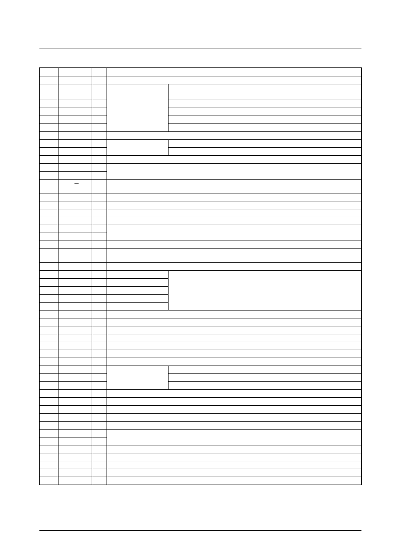
Pin Functions
No. 5811-7/27
LC78624E
Pin No.
Symbol
I/O
Function
1
DEFI
I
Defect detection signal (DEF) input. (Must be connected to 0 V when unused.)
2
TAI
I
Test input. A pull-down resistor is built in. Must be connected to 0 V.
3
PDO
O
External VCO control phase comparator output
4
VV
SS
ISET
–
PLL pins
Internal VCO ground. Must be connected to 0 V.
5
AI
PDO output current adjustment resistor connection
6
VV
DD
FR
–
Internal VCO power supply
7
AI
VCO frequency range adjustment
8
V
SS
EFMO
–
Digital system ground. Must be connected to 0 V.
9
O
Slice level control
EFM signal output
10
EFMIN
I
EFM signal input
11
TEST2
I
Test input. A pull-down resistor is built in. Must be connected to 0 V.
12
CLV
+
O
Disc motor control output.
Three-value output is also possible when specified by microcontroller command.
13
CLV
–
O
14
V/P
O
Rough servo/phase control automatic switching monitor output. Outputs a high level during rough servo and a low level
during phase control.
15
HFL
I
Track detection signal input. This is a Schmitt input.
16
TES
I
Tracking error signal input. This is a Schmitt input.
17
TOFF
O
Tracking off output
18
TGL
O
Tracking gain switching output. Increase the gain when low.
19
JP
+
O
Track jump control output.
Three-value output is also possible when specified by microcontroller command.
20
JP
–
O
21
PCK
O
EFM data playback clock monitor. Outputs 4.3218 MHz when the phase is locked.
22
FSEQ
O
Synchronization signal detection output. Outputs a high level when the synchronization signal detected from the EFM
signal and the internally generated synchronization signal agree.
23
V
DD
CONT1
–
Digital system power supply.
24
I/O
General-purpose I/O pin 1
25
CONT2
I/O
General-purpose I/O pin 2
Controlled by serial data commands from the microcontroller. Any of these that are unused
must be either set up as input ports and connected to 0 V, or set up as output ports and
left open.
26
CONT3
I/O
General-purpose I/O pin 3
27
CONT4
I/O
General-purpose I/O pin 4
28
CONT5
I/O
General-purpose I/O pin 5
29
EMPH
O
De-emphasis monitor pin. A high level indicates playback of a de-emphasis disk.
30
C2F
O
C2 flag output
31
DOUT
O
Digital output. (EIAJ format)
32
TEST3
I
Test input. A pull-down resistor is built in. Must be connected to 0 V.
33
TEST4
I
Test input. A pull-down resistor is built in. Must be connected to 0 V.
34
TEST6
I
Test input. A pull-down resistor is built in. Must be connected to 0 V.
35
TEST7
O
Test output
36
LRSY
O
L/R clock output
37
CK2
O
ROMXA output
Bit clock output
38
ROMXA
O
Interpolated data output, not ROM output
39
SRDT
O
Text data output
40
DQSY
O
Text readout enable output
41
SCLK
I
Text shift clock input
42
TEST8
O
Test output
43
XV
DD
X
OUT
X
IN
XV
SS
SBSY
–
Crystal oscillator power supply.
44
O
Connections for a 16.9344 crystal oscillator element
45
I
46
–
Crystal oscillator ground. Must be connected to 0 V.
47
O
Subcode block synchronization signal output
48
EFLG
O
C1, C2, single and double error correction monitor pin
49
PW
O
Subcode P, Q, R, S, T, U, V and W output
50
SFSY
O
Subcode frame synchronization signal output. This signal falls when the subcodes are in the standby state.
Continued on next page.
相關(guān)PDF資料 |
PDF描述 |
|---|---|
| LC78625E | SigmaDSP 28-/56-Bit Audio Processor with Two ADCs and Four DACs |
| LC78625 | SigmaDSP 28-/56-Bit Audio Processor with Two ADCs and Four DACs |
| LC78626KE | Compact Disc Player DSP(用于CD播放器的8位DSP) |
| LC78626 | 16-bit fixed point DSP with Flash |
| LC78626E | 16-bit fixed point DSP with Flash |
相關(guān)代理商/技術(shù)參數(shù) |
參數(shù)描述 |
|---|---|
| LC78625 | 制造商:SANYO 制造商全稱:Sanyo Semicon Device 功能描述:Compact Disc Player DSP |
| LC78625E | 制造商:SANYO 制造商全稱:Sanyo Semicon Device 功能描述:Compact Disc Player DSP |
| LC78626 | 制造商:SANYO 制造商全稱:Sanyo Semicon Device 功能描述:DSP for Compact Disk Players |
| LC78626E | 制造商:SANYO 制造商全稱:Sanyo Semicon Device 功能描述:DSP for Compact Disk Players |
| LC78626KE | 制造商:未知廠家 制造商全稱:未知廠家 功能描述:CD-Player Processor/Controller |
發(fā)布緊急采購,3分鐘左右您將得到回復(fù)。