- 您現(xiàn)在的位置:買賣IC網(wǎng) > PDF目錄43901 > L6995STR (STMICROELECTRONICS) SWITCHING CONTROLLER, PDSO20 PDF資料下載
參數(shù)資料
| 型號: | L6995STR |
| 廠商: | STMICROELECTRONICS |
| 元件分類: | 穩(wěn)壓器 |
| 英文描述: | SWITCHING CONTROLLER, PDSO20 |
| 封裝: | MO-153-AC, TSSOP-20 |
| 文件頁數(shù): | 24/26頁 |
| 文件大?。?/td> | 427K |
| 代理商: | L6995STR |
第1頁第2頁第3頁第4頁第5頁第6頁第7頁第8頁第9頁第10頁第11頁第12頁第13頁第14頁第15頁第16頁第17頁第18頁第19頁第20頁第21頁第22頁第23頁當(dāng)前第24頁第25頁第26頁
7/26
L6995S
quency after a load transient as well as to mask PWM comparator output against noise and spikes.
The system has not an internal clock, because this is a hysteretic controller, so the turn on pulse will start if three
conditions are met contemporarily: the FB pin voltage is lower than the reference voltage, the minimum off time
is passed and the current limit comparator is not triggered (i.e. the inductor current is below the current limit
value). The voltage on the OSC pin must range between 50mV and 2V to ensure the system linearity.
4.2 Closing the loop
The loop is closed connecting the output voltage (or the output divider middle point) to the FB pin. The FB pin
is linked internally to the comparator negative pin and the positive pin is connected to the reference voltage
(0.9V Typ.) as in Figure 2. When the FB goes lower than the reference voltage, the PWM comparator output
goes high and sets the flip-flop output, turning on the high side MOSFET. This condition is latched to avoid noise
spike. After the on-time (calculated as described in the previous section) the system resets the flip-flop and then
turns off the high side MOSFET and turns on the low side MOSFET. Internally the device has more complex
logic than a flip-flop to manage the transition in correct way. For more details refers to the Figure 3.
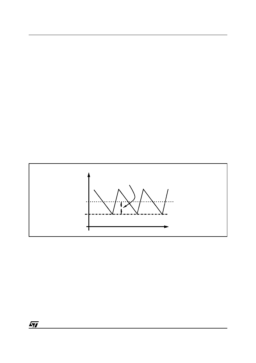
The voltage drop along ground and supply metals connecting output capacitor to the load is a source of DC
error. Further the system regulates the output voltage valley value not the average, as in the Figure 5 is shown.
So the voltage ripple on the output capacitor is a source of DC static error (as the PCB traces). To compensate
the DC errors, an integrator network must be introduced in the control loop, by connecting the output voltage to
the INT pin through a capacitor and the FB pin to the INT pin directly as in Figure 6. The internal integrator am-
plifier with the external capacitor CINT1 introduces a DC pole in the control loop. CINT1 also provides an AC path
for output ripple.
Figure 6. Valley regulation
The integrator amplifier generates a current, proportional to the DC errors, that increases the output capacitance
voltage in order to compensate the total static errors. A voltage clamper within the device forces INT pin voltage
ranges from VREF-50mV, VREF+150mV. This is useful to avoid or smooth output voltage overshoot during a load
transient. Also, this means that the integrator is capable of recovering output error due to ripple when its peak-
to-peak amplitude is less than 150mV in steady state.
In case of the ripple amplitude is larger than 150mV, a capacitor CINT2 can be connected between INT pin and
ground to reduce ripple amplitude at INT pin, otherwise the integrator can operate out of its linear range. Choose
CINT1 according to the following equation:
Eq 5
where GINT=50 s is the integrator transconductance,
αOUT is the output divider ratio given from Eq4 and FU
is the close loop bandwidth. This equation also holds if CINT2 is connected between INT pin and ground. CINT2
is given by:
Time
Vout
Vref
<Vout>
DC Error Offset
C
INT1
g
INT
α
OUT
2
π F
u
-------------------------------
=
相關(guān)PDF資料 |
PDF描述 |
|---|---|
| L6997D | SWITCHING CONTROLLER, PDSO20 |
| L6997DTR | SWITCHING CONTROLLER, PDSO20 |
| L7200 | DISK DRIVE MOTOR CONTROLLER, 2.6 A, PQFP64 |
| L7250 | VOICE COIL MOTOR CONTROLLER, PQFP64 |
| L7980A | 3.5 A SWITCHING REGULATOR, 1000 kHz SWITCHING FREQ-MAX, PDSO8 |
相關(guān)代理商/技術(shù)參數(shù) |
參數(shù)描述 |
|---|---|
| L6996 | 功能描述:DC/DC 開關(guān)控制器 Step-Down Contrllr RoHS:否 制造商:Texas Instruments 輸入電壓:6 V to 100 V 開關(guān)頻率: 輸出電壓:1.215 V to 80 V 輸出電流:3.5 A 輸出端數(shù)量:1 最大工作溫度:+ 125 C 安裝風(fēng)格: 封裝 / 箱體:CPAK |
| L6996-1 | 制造商:Johanson 功能描述:TUNING ROTOR |
| L6996-13 | 制造商:Johanson Manufacturing 功能描述:TUNING ELEMENT |
| L6996-16 | 制造商:Johanson Manufacturing 功能描述:TUNING ELEMENT |
| L6996-17 | 制造商:Johanson Manufacturing 功能描述:TUNING ELEMENT |
發(fā)布緊急采購,3分鐘左右您將得到回復(fù)。