- 您現(xiàn)在的位置:買賣IC網(wǎng) > PDF目錄43901 > L6918AD (STMICROELECTRONICS) SWITCHING CONTROLLER, 1200 kHz SWITCHING FREQ-MAX, PDSO28 PDF資料下載
參數(shù)資料
| 型號: | L6918AD |
| 廠商: | STMICROELECTRONICS |
| 元件分類: | 穩(wěn)壓器 |
| 英文描述: | SWITCHING CONTROLLER, 1200 kHz SWITCHING FREQ-MAX, PDSO28 |
| 封裝: | SO-28 |
| 文件頁數(shù): | 20/35頁 |
| 文件大?。?/td> | 431K |
| 代理商: | L6918AD |
第1頁第2頁第3頁第4頁第5頁第6頁第7頁第8頁第9頁第10頁第11頁第12頁第13頁第14頁第15頁第16頁第17頁第18頁第19頁當(dāng)前第20頁第21頁第22頁第23頁第24頁第25頁第26頁第27頁第28頁第29頁第30頁第31頁第32頁第33頁第34頁第35頁
27/35
L6918 L6918A
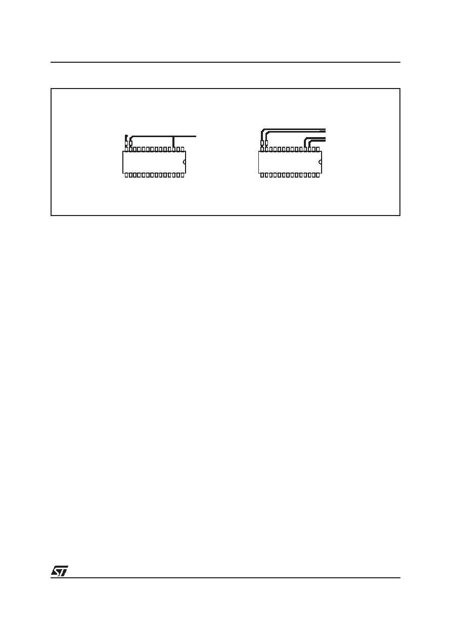
Figure 18. PCB layout connections for sense nets.
Interconnections between devices.
Master and Slave devices share reference and other signals for the regulation. To avoid noise injection into de-
vices, it is recommended to route these nets carefully.
– VPROG_IN / VPROG_OUT: This is the reference for the regulation. It must be routed far away from
any noisy trace and guarded by ground traces in order to avoid noise injection into the device. It can
be filtered with a 30nF maximum of distributed capacitance vs. signal ground.
– SLAVE_OK: This signal is used by the devices for the start-up synchronization and also to commu-
nicate UVP from Slave to Master device. It must be filtered by 1nF capacitor near the pin of each de-
vice to avoid the noise to cause false protection’s trigger.
Demo Board Description
The L6918 demo board shows the operation of the device in a four phases application. This evaluation board al-
lows output voltage adjustability (1.100V - 1.850V) through the switches S0-S4 and high output current capability.
The board has been laid out with the possibility to use up to two D2PACK mosfets for the low side switch in order
to give maximum flexibility in the mosfet choice.
The four layers demo board’s copper thickness is of 70
m in order to minimize conduction losses considering
the high current that the circuit is able to deliver.
Demo board schematic circuit is reported in Figure 19.
Several jumpers allow setting different configurations for the device: JP3, JP4 and JP5 allow configuring the
remote buffer as desired. Simply shorting JP4 and JP5 the remote buffer is enabled and it senses the output
voltage on-board; to implement a real remote sense, leave these jumpers open and connect the FBG and FBR
connectors on the demo board to the remote load. To avoid using the remote buffer, simply short all the jumpers
JP3, JP4 and JP5. Local sense through the R7 is used for the regulation.
The input can be configured in different ways using the jumpers JP1, JP2 and JP6; these jumpers control also
the mosfet driver supply voltage. Anyway, power conversion starts from VIN and the device is supplied from VCC
(See Figure 20).
NOT CORRECT
CORRECT
To PHASE
connection
VIA to GND plane
To HS Gate
and Source
To LS Drain
and Source
Wrong (left) and correct (right) connections for the current reading sensing nets.
相關(guān)PDF資料 |
PDF描述 |
|---|---|
| L6919CD | SWITCHING CONTROLLER, 200 kHz SWITCHING FREQ-MAX, PDSO28 |
| L6919E | SWITCHING CONTROLLER, PDSO28 |
| L6920DTR | 1.2 A SWITCHING REGULATOR, PDSO8 |
| L6920D | 1.2 A SWITCHING REGULATOR, PDSO8 |
| L6920 | 1.2 A SWITCHING REGULATOR, PDSO8 |
相關(guān)代理商/技術(shù)參數(shù) |
參數(shù)描述 |
|---|---|
| L6918ADTR | 功能描述:DC/DC 開關(guān)控制器 Prog Multi-Phase Cnt RoHS:否 制造商:Texas Instruments 輸入電壓:6 V to 100 V 開關(guān)頻率: 輸出電壓:1.215 V to 80 V 輸出電流:3.5 A 輸出端數(shù)量:1 最大工作溫度:+ 125 C 安裝風(fēng)格: 封裝 / 箱體:CPAK |
| L6918D | 功能描述:DC/DC 開關(guān)控制器 Prog Multi-Phase Cnt RoHS:否 制造商:Texas Instruments 輸入電壓:6 V to 100 V 開關(guān)頻率: 輸出電壓:1.215 V to 80 V 輸出電流:3.5 A 輸出端數(shù)量:1 最大工作溫度:+ 125 C 安裝風(fēng)格: 封裝 / 箱體:CPAK |
| L6918DTR | 功能描述:DC/DC 開關(guān)控制器 Prog Multi-Phase Cnt RoHS:否 制造商:Texas Instruments 輸入電壓:6 V to 100 V 開關(guān)頻率: 輸出電壓:1.215 V to 80 V 輸出電流:3.5 A 輸出端數(shù)量:1 最大工作溫度:+ 125 C 安裝風(fēng)格: 封裝 / 箱體:CPAK |
| L6919 | 制造商:未知廠家 制造商全稱:未知廠家 功能描述:5 BIT PROGRAMMABLE DUAL-PHASE CONTROLLER WITH DYNAMIC VID MANAGEMENT |
| L6919C | 制造商:STMICROELECTRONICS 制造商全稱:STMicroelectronics 功能描述:5 BIT PROGRAMMABLE DUAL-PHASE CONTROLLER WITH DYNAMIC VID MANAGEMENT |
發(fā)布緊急采購,3分鐘左右您將得到回復(fù)。