- 您現(xiàn)在的位置:買(mǎi)賣(mài)IC網(wǎng) > PDF目錄43901 > L6917D (STMICROELECTRONICS) SWITCHING CONTROLLER, 1000 kHz SWITCHING FREQ-MAX, PDSO28 PDF資料下載
參數(shù)資料
| 型號(hào): | L6917D |
| 廠商: | STMICROELECTRONICS |
| 元件分類(lèi): | 穩(wěn)壓器 |
| 英文描述: | SWITCHING CONTROLLER, 1000 kHz SWITCHING FREQ-MAX, PDSO28 |
| 封裝: | SO-28 |
| 文件頁(yè)數(shù): | 2/27頁(yè) |
| 文件大小: | 411K |
| 代理商: | L6917D |
第1頁(yè)當(dāng)前第2頁(yè)第3頁(yè)第4頁(yè)第5頁(yè)第6頁(yè)第7頁(yè)第8頁(yè)第9頁(yè)第10頁(yè)第11頁(yè)第12頁(yè)第13頁(yè)第14頁(yè)第15頁(yè)第16頁(yè)第17頁(yè)第18頁(yè)第19頁(yè)第20頁(yè)第21頁(yè)第22頁(yè)第23頁(yè)第24頁(yè)第25頁(yè)第26頁(yè)第27頁(yè)
L6917
10/27
Driver Section
The integrated high-current drivers allow using different types of power MOS (also multiple MOS to reduce the
RDSON), maintaining fast switching transition.
The drivers for the high-side mosfets use BOOTx pins for supply and PHASEx pins for return. The drivers for
the low-side mosfets use VCCDR pin for supply and PGND pin for return. A minimum voltage of 4.6V at VCCDR
pin is required to start operations of the device.
The controller embodies a sophisticated anti-shoot-through system to minimize low side body diode conduction
time maintaining good efficiency and saving the use of Schottky diodes. The dead time is reduced to few nano-
seconds assuring that high-side and low-side mosfets are never switched on simultaneously: when the high-
side mosfet turns off, the voltage on its source begins to fall; when the voltage reaches 2V, the low-side mosfet
gate drive is applied with 30ns delay. When the low-side mosfet turns off, the voltage at LGATEx pin is sensed.
When it drops below 1V, the high-side mosfet gate drive is applied with a delay of 30ns.
If the current flowing in the inductor is negative, the source of high-side mosfet will never drop. To allow the turn-
ing on of the low-side mosfet even in this case, a watchdog controller is enabled: after 240ns, the low side mos-
fet is switched on so allowing the negative current of the inductor to recirculate. This mechanism allows the
system to regulate even if the current is negative.
The BOOTx and VCCDR pins are separated from IC’s power supply (VCC pin) as well as signal ground (SGND
pin) and power ground (PGND pin) in order to maximize the switching noise immunity. The separated supply
for the different drivers gives high flexibility in mosfet choice, allowing the use of logic-level mosfet. Several com-
bination of supply can be chosen to optimize performance and efficiency of the application. Power conversion
is also flexible, 5V or 12V bus can be chosen freely.
Placement of the power mosfets is critical: long and narrow trace length from UGATEx and LGATEx pins to the
mosfets’ gates may cause high amount of ringing due to the resonance between inductance of the trace and
the gate capacitance of the mosfet. A gate resistance of a few ohms can help in reducing ringing and power
dissipation of the controller without compromising system efficiency.
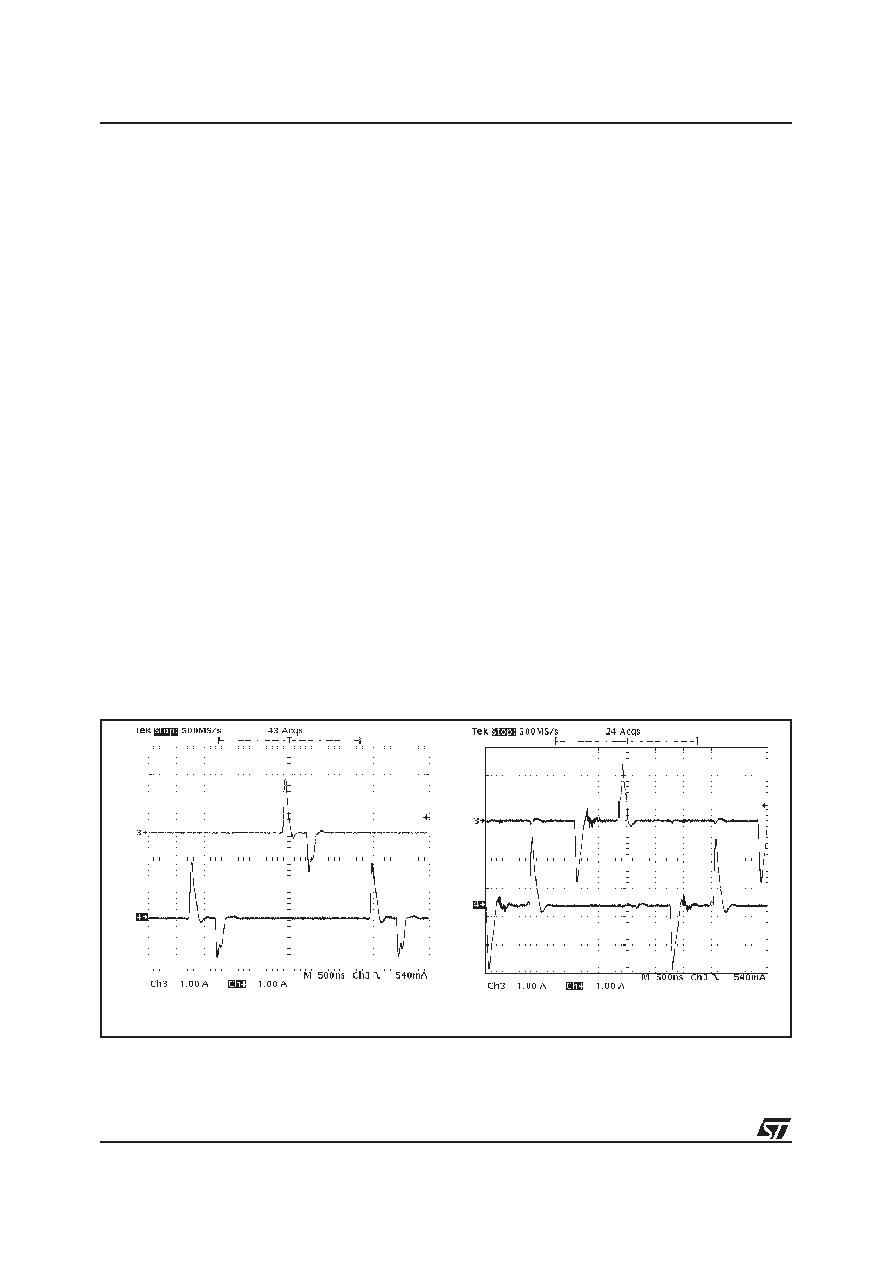
The peak current is shown for both the upper and the lower driver of the two phases in figure 3. A 10nF capac-
itive load has been used. For the upper drivers, the source current is 1.9A while the sink current is 1.5A with
VBOOT-VPHASE = 12V; similarly, for the lower drivers, the source current is 2.4A while the sink current is 2A with
VCCDR = 12V.
Figure 3. Drivers peak current: High Side (left) and Low Side (right)
CH3 = HGATE1; CH4 = HGATE2
CH3 = LGATE1; CH4 = LGATE2
相關(guān)PDF資料 |
PDF描述 |
|---|---|
| L6918ADTR | SWITCHING CONTROLLER, 1200 kHz SWITCHING FREQ-MAX, PDSO28 |
| L6918AD | SWITCHING CONTROLLER, 1200 kHz SWITCHING FREQ-MAX, PDSO28 |
| L6919CD | SWITCHING CONTROLLER, 200 kHz SWITCHING FREQ-MAX, PDSO28 |
| L6919E | SWITCHING CONTROLLER, PDSO28 |
| L6920DTR | 1.2 A SWITCHING REGULATOR, PDSO8 |
相關(guān)代理商/技術(shù)參數(shù) |
參數(shù)描述 |
|---|---|
| L6917DTR | 制造商:未知廠家 制造商全稱:未知廠家 功能描述:Analog IC |
| L6918 | 制造商:STMICROELECTRONICS 制造商全稱:STMicroelectronics 功能描述:5 BIT PROGRAMMABLE MULTIPHASE CONTROLLER |
| L6918A | 制造商:STMICROELECTRONICS 制造商全稱:STMicroelectronics 功能描述:5 BIT PROGRAMMABLE MULTIPHASE CONTROLLER |
| L6918AD | 功能描述:DC/DC 開(kāi)關(guān)控制器 Prog Multi-Phase Cnt RoHS:否 制造商:Texas Instruments 輸入電壓:6 V to 100 V 開(kāi)關(guān)頻率: 輸出電壓:1.215 V to 80 V 輸出電流:3.5 A 輸出端數(shù)量:1 最大工作溫度:+ 125 C 安裝風(fēng)格: 封裝 / 箱體:CPAK |
| L6918ADTR | 功能描述:DC/DC 開(kāi)關(guān)控制器 Prog Multi-Phase Cnt RoHS:否 制造商:Texas Instruments 輸入電壓:6 V to 100 V 開(kāi)關(guān)頻率: 輸出電壓:1.215 V to 80 V 輸出電流:3.5 A 輸出端數(shù)量:1 最大工作溫度:+ 125 C 安裝風(fēng)格: 封裝 / 箱體:CPAK |
發(fā)布緊急采購(gòu),3分鐘左右您將得到回復(fù)。