- 您現(xiàn)在的位置:買賣IC網(wǎng) > PDF目錄296260 > K8S1215EZC-SC1C0 32M X 16 FLASH 1.8V PROM, 100 ns, PBGA64 PDF資料下載
參數(shù)資料
| 型號: | K8S1215EZC-SC1C0 |
| 元件分類: | PROM |
| 英文描述: | 32M X 16 FLASH 1.8V PROM, 100 ns, PBGA64 |
| 封裝: | 9 X 11 MM, 1 MM HEIGHT, 0.50 MM PITCH, LEAD FREE, FBGA-64 |
| 文件頁數(shù): | 45/83頁 |
| 文件大小: | 1511K |
| 代理商: | K8S1215EZC-SC1C0 |
第1頁第2頁第3頁第4頁第5頁第6頁第7頁第8頁第9頁第10頁第11頁第12頁第13頁第14頁第15頁第16頁第17頁第18頁第19頁第20頁第21頁第22頁第23頁第24頁第25頁第26頁第27頁第28頁第29頁第30頁第31頁第32頁第33頁第34頁第35頁第36頁第37頁第38頁第39頁第40頁第41頁第42頁第43頁第44頁當(dāng)前第45頁第46頁第47頁第48頁第49頁第50頁第51頁第52頁第53頁第54頁第55頁第56頁第57頁第58頁第59頁第60頁第61頁第62頁第63頁第64頁第65頁第66頁第67頁第68頁第69頁第70頁第71頁第72頁第73頁第74頁第75頁第76頁第77頁第78頁第79頁第80頁第81頁第82頁第83頁

- 5 -
K8S1215E(T/B/Z)C
datasheet NOR FLASH MEMORY
Rev. 1.1
512M Bit (32M x16) Muxed Burst / Multi Bank SLC NOR Flash Memory
1.0 FEATURES
Single Voltage, 1.7V to 1.95V for Read and Write operations
Organization
- 33,554,432 x 16 bit (Word Mode Only)
Multiplexed Data and Address for reduction of interconnections
- A/DQ0 ~ A/DQ15
Read While Program/Erase Operation
Multiple Bank Architecture
- 16 Banks (32Mb Partition)
OTP Block : Extra 512-Word block
Read Access Time (@ CL=30pF)
- Asynchronous Random Access Time : 100ns
- Synchronous Random Access Time : 95ns
- Burst Access Time :
11ns (66MHz) / 9ns (83MHz) / 7ns (108MHz) /6ns (133MHz)
Burst Length :
- Continuous Linear Burst
- Linear Burst : 8-word & 16-word with Wrap
Block Architecture
- Uniform block part (K8S(10/11/12/13)15EZC) :
Five hundred twelve 64Kword blocks
- Boot block part (K8S(10/11/12/13)15ET(B)C) :
Four 16Kword blocks and five hundred eleven 64Kword blocks (Bank 0
contains four 16 Kword blocks and thirty-one 64Kword blocks, Bank 1 ~
Bank 15 contain four hundred eighty 64Kword blocks)
Reduce program time using the VPP
Support 512-word Buffer Program
Power Consumption (Typical value, CL=30pF)
- Synchronous Read Current : 35mA at 133MHz
- Program/Erase Current : 25mA
- Read While Program/Erase Current : 45mA
- Standby Mode/Auto Sleep Mode : 30uA
Block Protection/Unprotection
- Using the software command sequence
- Last two boot blocks are protected by WP=VIL
(Boot block part : K8S(10/11/12/13)15ET(B)C)
- Last one block (BA511) is protected by WP=VIL
(Uniform block part : K8S(10/11/12/13)15EZC)
- All blocks are protected by VPP=VIL
Handshaking Feature
- Provides host system with minimum latency by monitoring RDY
Erase Suspend/Resume
Program Suspend/Resume
Unlock Bypass Program/Erase
Blank Check Feature
Hardware Reset (RESET)
Deep Power Down Mode
Data Polling and Toggle Bits
- Provides a software method of detecting the status of program
or erase completion
Endurance
- 100K Program/Erase cycles
Extended Temperature : -25°C ~ 85°C
Support Common Flash Memory Interface
Low Vcc Write Inhibit
Output Driver Control by Configuration Register
Package : 64Ball FBGA type (9mm x 11mm), 0.5mm ball pitch
1.0mm(Max.)Thickness
2.0 GENERAL DESCRIPTION
The K8S(10/11/12/13)15E featuring single 1.8V power supply is a 512Mbit
Muxed Burst Multi Bank Flash Memory organized as 32Mx16. The memory
architecture of the device is designed to divide its memory arrays into
512blocks(Uniform block part)/515 blocks (Boot block part) with indepen-
dent hardware protection. This block architecture provides highly flexible
erase and program capability. The K8S(10/11/12/13)15E NOR Flash con-
sists of sixteen banks. This device is capable of reading data from one bank
while programming or erasing in the other bank. Regarding read access
time, the K8S10/1215E provides an 11ns burst access time and an 95ns
initial access time at 66MHz. At 83MHz, the K8S10/1215E provides an 9ns
burst access time and an 95ns initial access time. At 108MHz, the K8S11/
1315E provides an 7ns burst access time and an 95ns initial access time.
At 133MHz, the K8S11/1315E provides an 6ns burst access time and an
95ns initial access time. The device performs a program operation in units
of 16 bits (Word) and erases in units of a block. Single or multiple blocks
can be erased. The block erase operation is completed within typically
0.6sec. The device requires 25mA as program/erase current in the
extended temperature ranges.
The K8S(10/11/12/13)15E NOR Flash Memory is created by using Sam-
sung's advanced CMOS process technology.
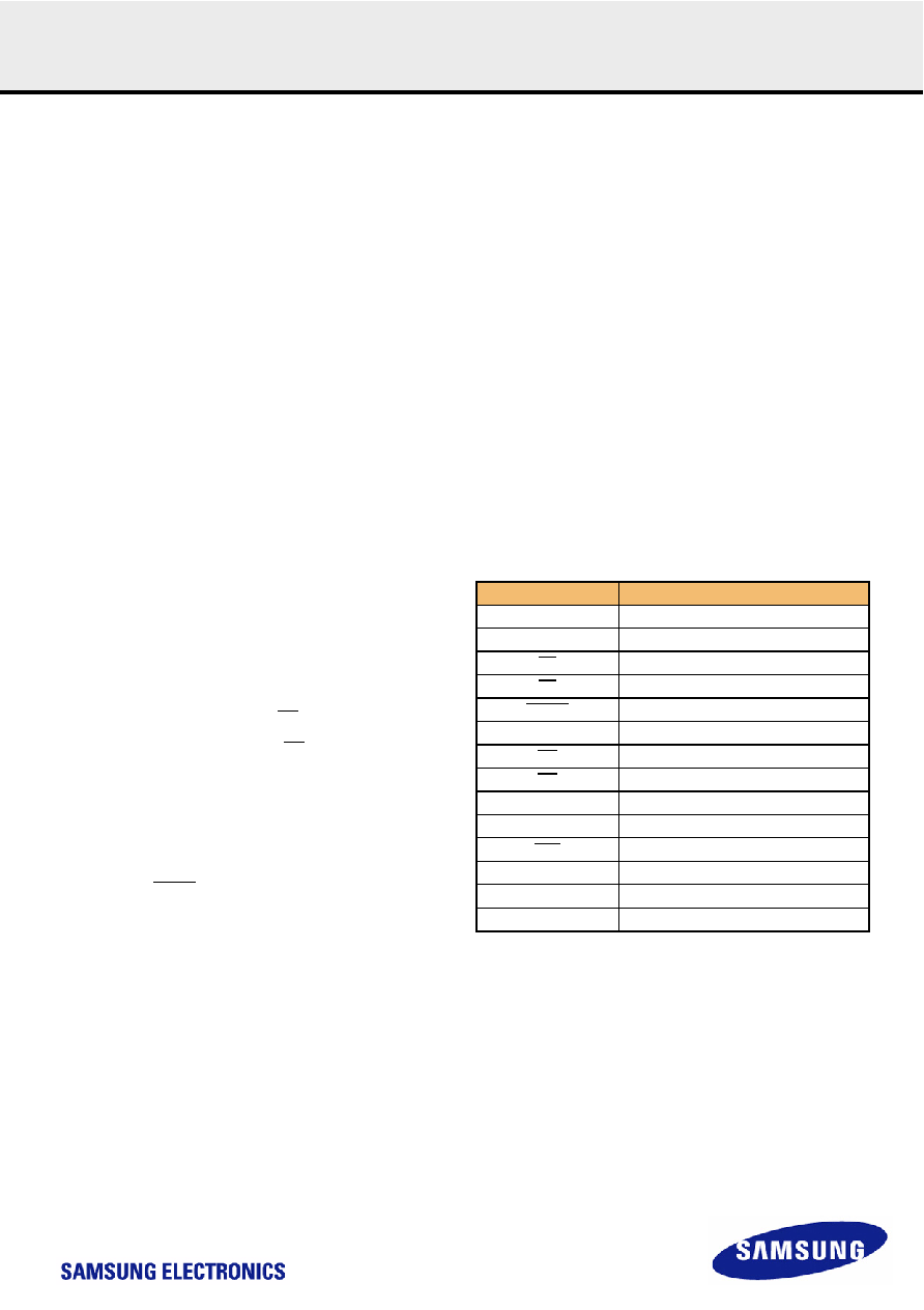
3.0 PIN DESCRIPTION
Pin Name
Pin Function
A16 - A24
Address Inputs
A/DQ0 - A/DQ15
Multiplexed Address/Data input/output
CE
Chip Enable
OE
Output Enable
RESET
Hardware Reset
VPP
Accelerates Programming
WE
Write Enable
WP
Hardware Write Protection Input
CLK
Clock
RDY
Ready Output
AVD
Address Valid Input
DPD
Deep Power Down
Vcc
Power Supply
VSS
Ground
相關(guān)PDF資料 |
PDF描述 |
|---|---|
| K8S5515ETC-SC1E0 | 16M X 16 FLASH 1.8V PROM, 100 ns, PBGA44 |
| K9E2G08U0M-YIB00 | 256M X 8 FLASH 2.7V PROM, 30 ns, PDSO48 |
| KA-59-281 | TNC CONNECTOR, PLUG |
| KA-91-02 | RF STRAIGHT ADAPTER |
| KA-91-16 | RF TEE ADAPTER |
相關(guān)代理商/技術(shù)參數(shù) |
參數(shù)描述 |
|---|---|
| K8S2815ETE | 制造商:SAMSUNG 制造商全稱:Samsung semiconductor 功能描述:128Mb E-die NOR FLASH |
| K8S5615ETC | 制造商:SAMSUNG 制造商全稱:Samsung semiconductor 功能描述:256Mb C-die NOR Flash |
| K8S6415EBB-DC7C | 制造商:SAMSUNG 制造商全稱:Samsung semiconductor 功能描述:64M Bit (4M x16) Muxed Burst , Multi Bank NOR Flash Memory |
| K8S6415EBB-DE7C | 制造商:SAMSUNG 制造商全稱:Samsung semiconductor 功能描述:64M Bit (4M x16) Muxed Burst , Multi Bank NOR Flash Memory |
| K8S6415EBB-FC7C | 制造商:SAMSUNG 制造商全稱:Samsung semiconductor 功能描述:64M Bit (4M x16) Muxed Burst , Multi Bank NOR Flash Memory |
發(fā)布緊急采購,3分鐘左右您將得到回復(fù)。