- 您現(xiàn)在的位置:買賣IC網(wǎng) > PDF目錄374284 > K4T51043QC-ZCLE6 (SAMSUNG SEMICONDUCTOR CO. LTD.) 512Mb C-die DDR2 SDRAM PDF資料下載
參數(shù)資料
| 型號(hào): | K4T51043QC-ZCLE6 |
| 廠商: | SAMSUNG SEMICONDUCTOR CO. LTD. |
| 英文描述: | 512Mb C-die DDR2 SDRAM |
| 中文描述: | 葷的512Mb芯片DDR2內(nèi)存 |
| 文件頁數(shù): | 22/29頁 |
| 文件大小: | 629K |
| 代理商: | K4T51043QC-ZCLE6 |
第1頁第2頁第3頁第4頁第5頁第6頁第7頁第8頁第9頁第10頁第11頁第12頁第13頁第14頁第15頁第16頁第17頁第18頁第19頁第20頁第21頁當(dāng)前第22頁第23頁第24頁第25頁第26頁第27頁第28頁第29頁
Page 22 of 29
Rev. 1.4 Aug. 2005
DDR2 SDRAM
512Mb C-die DDR2 SDRAM
General notes, which may apply for all AC parameters
1. Slew Rate Measurement Levels
a. Output slew rate for falling and rising edges is measured between VTT - 250 mV and VTT + 250 mV for
single ended signals. For differential signals (e.g. DQS - DQS) output slew rate is measured between DQS - DQS = -500 mV and DQS - DQS =
+500mV. Output slew rate is guaranteed by design, but is not necessarily tested on each device.
b. Input slew rate for single ended signals is measured from dc-level to ac-level: from VIL(dc) to VIH(ac) for rising edges and from VIH(dc) and VIL(ac)
for falling edges.
For differential signals (e.g. CK - CK) slew rate for rising edges is measured from CK - CK = -250 mV to CK - CK = +500 mV
(250mV to -500 mV for
falling edges).
c. VID is the magnitude of the difference between the input voltage on CK and the input voltage on CK, or between DQS and DQS for differential
strobe.
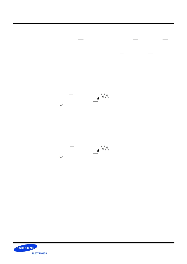
2. DDR2 SDRAM AC timing reference load
Following figure represents the timing reference load used in defining the relevant timing parameters of the part. It is not intended to be either a precise
representation of the typical system environment or a depiction of the actual load presented by a production tester. System designers will use IBIS or other
simulation tools to correlate the timing reference load to a system environment. Manufacturers will correlate to their production test conditions (generally a
coaxial transmission line terminated at the tester electronics).
The output timing reference voltage level for single ended signals is the crosspoint with VTT. The output timing reference voltage level for differential sig-
nals is the crosspoint of the true (e.g. DQS) and the complement (e.g. DQS) signal.
3. DDR2 SDRAM output slew rate test load
Output slew rate is characterized under the test conditions as shown in the following figure.
VDDQ
DUT
DQ
DQS
DQS
RDQS
RDQS
Output
V
TT
= V
DDQ
/2
25
Timing
reference
point
<AC Timing Reference Load>
VDDQ
DUT
DQ
DQS, DQS
RDQS, RDQS
Output
V
TT
= V
DDQ
/2
25
Test point
<Slew Rate Test Load>
相關(guān)PDF資料 |
PDF描述 |
|---|---|
| K4T51043QC-ZCD5 | 512Mb C-die DDR2 SDRAM |
| K4 | KS SERIES KEY SWITCHES |
| K5-C | Adjustable Type Coils |
| K5-N | Adjustable Type Coils |
| K5-N1 | Adjustable Type Coils |
相關(guān)代理商/技術(shù)參數(shù) |
參數(shù)描述 |
|---|---|
| K4T51043QC-ZLCC | 制造商:SAMSUNG 制造商全稱:Samsung semiconductor 功能描述:512Mb C-die DDR2 SDRAM |
| K4T51043QC-ZLD5 | 制造商:SAMSUNG 制造商全稱:Samsung semiconductor 功能描述:512Mb C-die DDR2 SDRAM |
| K4T51043QC-ZLE6 | 制造商:SAMSUNG 制造商全稱:Samsung semiconductor 功能描述:512Mb C-die DDR2 SDRAM |
| K4T51043QC-ZLE7 | 制造商:SAMSUNG 制造商全稱:Samsung semiconductor 功能描述:512Mb C-die DDR2 SDRAM |
| K4T51043QE | 制造商:SAMSUNG 制造商全稱:Samsung semiconductor 功能描述:512Mb E-die DDR2 SDRAM Specification |
發(fā)布緊急采購,3分鐘左右您將得到回復(fù)。