- 您現(xiàn)在的位置:買賣IC網(wǎng) > PDF目錄374284 > K4T51043QC-ZCD5 (SAMSUNG SEMICONDUCTOR CO. LTD.) 512Mb C-die DDR2 SDRAM PDF資料下載
參數(shù)資料
| 型號(hào): | K4T51043QC-ZCD5 |
| 廠商: | SAMSUNG SEMICONDUCTOR CO. LTD. |
| 英文描述: | 512Mb C-die DDR2 SDRAM |
| 中文描述: | 葷的512Mb芯片DDR2內(nèi)存 |
| 文件頁數(shù): | 23/29頁 |
| 文件大小: | 629K |
| 代理商: | K4T51043QC-ZCD5 |
第1頁第2頁第3頁第4頁第5頁第6頁第7頁第8頁第9頁第10頁第11頁第12頁第13頁第14頁第15頁第16頁第17頁第18頁第19頁第20頁第21頁第22頁當(dāng)前第23頁第24頁第25頁第26頁第27頁第28頁第29頁
Page 23 of 29
Rev. 1.4 Aug. 2005
DDR2 SDRAM
512Mb C-die DDR2 SDRAM
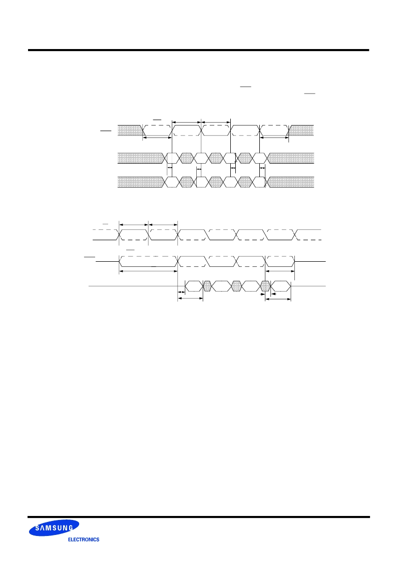
4. Differential data strobe
DDR2 SDRAM pin timings are specified for either single ended mode or differential mode depending on the setting of the EMRS “Enable DQS” mode
bit; timing advantages of differential mode are realized in system design. The method by which the DDR2 SDRAM pin timings are measured is mode
dependent. In single ended mode, timing relationships are measured relative to the rising or falling edges of DQS crossing at VREF. In differential mode,
these timing relationships are measured relative to the crosspoint of DQS and its complement, DQS. This distinction in timing methods is guaranteed by
design and characterization. Note that when differential data strobe mode is disabled via the EMRS, the complementary pin, DQS, must be tied externally
to VSS through a 20 ohm
to 10 K ohm
resisor to insure proper operation.
5. AC timings are for linear signal transitions.
6. These parameters guarantee device behavior, but they are not necessarily tested on each device. They
tester correlation.
may be guaranteed by device design or
7. All voltages are referenced to VSS.
8. Tests for AC timing, IDD, and electrical (AC and DC) characteristics, may be conducted at nominal reference/supply voltage levels, but the related
specifications and device operation are guaranteed for the full voltage range specified.
t
DS
t
DS
t
DH
t
WPRE
t
WPST
t
DQSH
t
DQSL
DQS
DQS
D
DMin
DQS/
DQS
DQ
DM
t
DH
<Data input (write) timing>
DMin
DMin
DMin
D
D
D
V
IL
(ac)
V
IH
(ac)
V
IL
(ac)
V
IH
(ac)
V
IL
(dc)
V
IH
(dc)
V
IL
(dc)
V
IH
(dc)
t
CH
t
CL
CK
CK
CK/CK
DQS/DQS
DQ
DQS
DQS
t
RPST
Q
t
RPRE
t
DQSQmax
t
QH
t
QH
t
DQSQmax
<Data output (read) timing>
Q
Q
Q
相關(guān)PDF資料 |
PDF描述 |
|---|---|
| K4 | KS SERIES KEY SWITCHES |
| K5-C | Adjustable Type Coils |
| K5-N | Adjustable Type Coils |
| K5-N1 | Adjustable Type Coils |
| K5-R2 | Adjustable Type Coils |
相關(guān)代理商/技術(shù)參數(shù) |
參數(shù)描述 |
|---|---|
| K4T51043QC-ZCD6 | 制造商:SAMSUNG 制造商全稱:Samsung semiconductor 功能描述:512Mb C-die DDR2 SDRAM |
| K4T51043QC-ZCE6 | 制造商:SAMSUNG 制造商全稱:Samsung semiconductor 功能描述:512Mb C-die DDR2 SDRAM |
| K4T51043QC-ZCE7 | 制造商:SAMSUNG 制造商全稱:Samsung semiconductor 功能描述:512Mb C-die DDR2 SDRAM |
| K4T51043QC-ZCLCC | 制造商:SAMSUNG 制造商全稱:Samsung semiconductor 功能描述:512Mb C-die DDR2 SDRAM |
| K4T51043QC-ZCLD5 | 制造商:SAMSUNG 制造商全稱:Samsung semiconductor 功能描述:512Mb C-die DDR2 SDRAM |
發(fā)布緊急采購,3分鐘左右您將得到回復(fù)。