- 您現(xiàn)在的位置:買賣IC網(wǎng) > PDF目錄373065 > K4N56163QF-GC25 (SAMSUNG SEMICONDUCTOR CO. LTD.) 256Mbit gDDR2 SDRAM PDF資料下載
參數(shù)資料
| 型號: | K4N56163QF-GC25 |
| 廠商: | SAMSUNG SEMICONDUCTOR CO. LTD. |
| 英文描述: | 256Mbit gDDR2 SDRAM |
| 中文描述: | 片256Mbit GDDR2 SDRAM的 |
| 文件頁數(shù): | 68/73頁 |
| 文件大小: | 1262K |
| 代理商: | K4N56163QF-GC25 |
第1頁第2頁第3頁第4頁第5頁第6頁第7頁第8頁第9頁第10頁第11頁第12頁第13頁第14頁第15頁第16頁第17頁第18頁第19頁第20頁第21頁第22頁第23頁第24頁第25頁第26頁第27頁第28頁第29頁第30頁第31頁第32頁第33頁第34頁第35頁第36頁第37頁第38頁第39頁第40頁第41頁第42頁第43頁第44頁第45頁第46頁第47頁第48頁第49頁第50頁第51頁第52頁第53頁第54頁第55頁第56頁第57頁第58頁第59頁第60頁第61頁第62頁第63頁第64頁第65頁第66頁第67頁當前第68頁第69頁第70頁第71頁第72頁第73頁
- 68 -
Rev 1.6 (Apr. 2005)
256M gDDR2 SDRAM
K4N56163QF-GC
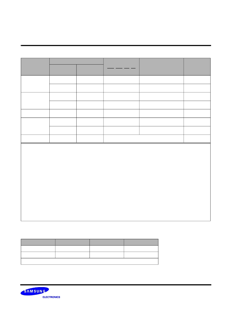
Clock Enable (CKE) Truth Table for Synchronous Transitions
Current State
2
CKE
Command (N)
3
RAS, CAS, WE, CS
Action (N)
3
Notes
Previous Cycle
1
(N-1)
Current Cycle
1
(N)
Power Down
L
L
X
Maintain Power-Down
11, 13, 15
L
H
DESELECT or NOP
Power Down Exit
4, 8, 11,13
Self Refresh
L
L
X
Maintain Self Refresh
11, 15
L
H
DESELECT or NOP
Self Refresh Exit
4, 5,9
Bank(s) Active
H
L
DESELECT or NOP
Active Power Down Entry
4,8,10,11,13
All Banks Idle
H
L
DESELECT or NOP
Precharge Power Down Entry
4, 8, 10,11,13
H
L
REFRESH
Self Refresh Entry
6, 9, 11,13
H
H
Refer to the Command Truth Table
7
Notes:
1. CKE (N) is the logic state of CKE at clock edge N; CKE (N–1) was the state of CKE at the previous clock edge.
2. Current state is the state of the DDR SDRAM immediately prior to clock edge N.
3. COMMAND (N) is the command registered at clock edge N, and ACTION (N) is a result of COMMAND (N).
4. All states and sequences not shown are illegal or reserved unless explicitly described elsewhere in this document.
5. On Self Refresh Exit DESELECT or NOP commands must be issued on every clock edge occurring during the t
XSNR
period. Read commands may
be issued only after t
XSRD
(200 clocks) is satisfied.
6. Self Refresh mode can only be entered from the All Banks Idle state.
7. Must be a legal command as defined in the Command Truth Table.
8. Valid commands for Power Down Entry and Exit are NOP and DESELECT only.
9. Valid commands for Self Refresh Exit are NOP and DESELECT only.
10. Power Down and Self Refresh can not be entered while Read or Write operations, (Extended) Mode Register Set operations or Precharge opera-
tions are in progress. See section "Power Down" and "Self Refresh Command" for a detailed list of restrictions.
11. Minimum CKE high time is three clocks.; minimum CKE low time is three clocks.
12. The state of ODT does not affect the states described in this table. The ODT function is not available during Self Refresh.
13. The Power Down does not perform any refresh operations. The duration of Power Down Mode is therefore limited by the refresh requirements out-
lined.
14. CKE must be maintained high while the SDRAM is in OCD calibration mode .
15. “X” means “don’t care (including floating around VREF)” in Self Refresh and Power Down. However ODT must be driven high or low in Power
Down if the ODT function is enabled (Bit A2 or A6 set to “1” in EMRS(1) ).
16. V
REF
must be maintained during Self Refresh operation.
DM Truth Table
Name (Functional)
DM
DQs
Note
Write enable
-
Valid
1
Write inhibit
H
X
1
1. Used to mask write data, provided coincident with the corresponding data
相關PDF資料 |
PDF描述 |
|---|---|
| K4N56163QF-GC30 | 256Mbit gDDR2 SDRAM |
| K4N56163QF-GC37 | 256Mbit gDDR2 SDRAM |
| K4PE68A | Transient Voltage Suppressor Diodes |
| K4R271669A | 256K x 16/18 bit x 2*16 Dependent Banks Direct RDRAMTM |
| K4R271669A-N(M)CK7 | 256K x 16/18 bit x 2*16 Dependent Banks Direct RDRAMTM |
相關代理商/技術參數(shù) |
參數(shù)描述 |
|---|---|
| K4N56163QF-GC30 | 制造商:SAMSUNG 制造商全稱:Samsung semiconductor 功能描述:256Mbit gDDR2 SDRAM |
| K4N56163QF-GC37 | 制造商:SAMSUNG 制造商全稱:Samsung semiconductor 功能描述:256Mbit gDDR2 SDRAM |
| K4N56163QG-ZC2A | 制造商:Samsung Semiconductor 功能描述: |
| K4P24V3 | 制造商:AROMAT 功能描述:REPLAY 700 OHM |
| K4P-24V-3 | 制造商:AROMAT 功能描述:REPLAY 700 OHM |
發(fā)布緊急采購,3分鐘左右您將得到回復。