- 您現(xiàn)在的位置:買賣IC網(wǎng) > PDF目錄374273 > K4H560438D-GCA2 (SAMSUNG SEMICONDUCTOR CO. LTD.) DDR 256Mb PDF資料下載
參數(shù)資料
| 型號: | K4H560438D-GCA2 |
| 廠商: | SAMSUNG SEMICONDUCTOR CO. LTD. |
| 英文描述: | DDR 256Mb |
| 中文描述: | 的DDR 256Mb的 |
| 文件頁數(shù): | 8/26頁 |
| 文件大?。?/td> | 291K |
| 代理商: | K4H560438D-GCA2 |
- 8 -
256Mb
DDR SDRAM
Rev. 2.2 Mar. ’03
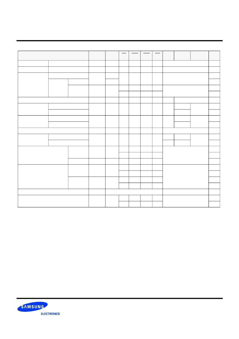
(V=Valid, X=Don
′
t Care, H=Logic High, L=Logic Low)
COMMAND
CKEn-1
CKEn
CS
RAS
CAS
WE
BA
0,1
A
10
/AP
A
11,
A
12
A
9
~ A
0
Note
Register
Extended MRS
H
X
L
L
L
L
OP CODE
1, 2
Register
Mode Register Set
H
X
L
L
L
L
OP CODE
1, 2
Refresh
Auto Refresh
H
H
L
L
L
H
X
3
Self
Refresh
Entry
L
3
Exit
L
H
L
H
H
H
X
3
H
X
X
X
3
Bank Active & Row Address
H
X
L
L
H
H
V
Row Address
Read &
Column Address
Auto Precharge Disable
H
X
L
H
L
H
V
L
Column
Address
4
Auto Precharge Enable
H
4
Write &
Column Address
Auto Precharge Disable
H
X
L
H
L
L
V
L
Column
Address
4
Auto Precharge Enable
H
4, 6
Burst Stop
H
X
L
H
H
L
X
7
Precharge
Bank Selection
H
X
L
L
H
L
V
L
X
All Banks
X
H
5
Active Power Down
Entry
H
L
H
X
X
X
X
L
V
V
V
Exit
L
H
X
X
X
X
Precharge Power Down Mode
Entry
H
L
H
X
X
X
X
L
H
H
H
Exit
L
H
H
X
X
X
L
V
V
V
DM
H
X
X
8
No operation (NOP) : Not defined
H
X
H
X
X
X
X
9
L
H
H
H
9
1. OP Code : Operand Code. A
0
~ A
12
& BA
0
~ BA
1
: Program keys. (@EMRS/MRS)
2.EMRS/ MRS can be issued only at all banks precharge state.
A new command can be issued 2 clock cycles after EMRS or MRS.
3. Auto refresh functions are same as the CBR refresh of DRAM.
The automatical precharge without row precharge command is meant by "Auto".
Auto/self refresh can be issued only at all banks precharge state.
4. BA
0
~ BA
1
: Bank select addresses.
If both BA
0
and BA
1
are "Low" at read, write, row active and precharge, bank A is selected.
If BA
0
is "High" and BA
1
is "Low" at read, write, row active and precharge, bank B is selected.
If BA
0
is "Low" and BA
1
is "High" at read, write, row active and precharge, bank C is selected.
If both BA
0
and BA
1
are "High" at read, write, row active and precharge, bank D is selected.
5. If A
10
/AP is "High" at row precharge, BA
0
and BA
1
are ignored and all banks are selected.
6. During burst write with auto precharge, new read/write command can not be issued.
Another bank read/write command can be issued after the end of burst.
New row active of the associated bank can be issued at t
RP
after the end of burst.
7. Burst stop command is valid at every burst length.
8. DM sampled at the rising and falling edges of the DQS and Data-in are masked at the both edges (Write DM latency is 0).
9. This combination is not defined for any function, which means "No Operation(NOP)" in DDR SDRAM.
相關(guān)PDF資料 |
PDF描述 |
|---|---|
| K4H560438D-GCB0 | DDR 256Mb |
| K4H560438D-GCB3 | DDR 256Mb |
| K4H560438D-GLA2 | DDR 256Mb |
| K4H560438E-ZLB0 | Connector Kit; Contents Of Kit:C14610F0240001 24 position bulkhead housing double latch, C14610B0241021 24 position female insert wire protect, Without spring cover; For Use With:C146 Heavy Duty Industrial Connectors RoHS Compliant: Yes |
| K4H560438E-ZLB3 | Connector Kit; Contents Of Kit:C14610G0245001 24 position hood PG 21 double latch low profile side entry, C14610A0241021 24 position male insert wire protect, VN162100014 PG 21 gland bushing, For 0.433" - 0.866" diameter cable RoHS Compliant: Yes |
相關(guān)代理商/技術(shù)參數(shù) |
參數(shù)描述 |
|---|---|
| K4H560438D-GCB0 | 制造商:SAMSUNG 制造商全稱:Samsung semiconductor 功能描述:DDR 256Mb |
| K4H560438D-GCB3 | 制造商:Samsung Semiconductor 功能描述:DRAM Chip DDR SDRAM 256M-Bit 64Mx4 2.5V 60-Pin FBGA Tray |
| K4H560438D-GLA2 | 制造商:SAMSUNG 制造商全稱:Samsung semiconductor 功能描述:DDR 256Mb |
| K4H560438D-GLB0 | 制造商:SAMSUNG 制造商全稱:Samsung semiconductor 功能描述:DDR 256Mb |
| K4H560438D-GLB3 | 制造商:SAMSUNG 制造商全稱:Samsung semiconductor 功能描述:DDR 256Mb |
發(fā)布緊急采購,3分鐘左右您將得到回復。