- 您現(xiàn)在的位置:買(mǎi)賣(mài)IC網(wǎng) > PDF目錄384545 > ISPPAC-CLK5610V-01TN48C (LATTICE SEMICONDUCTOR CORP) LED Ring Light; LED Color:Infrared; Leaded Process Compatible:No; Peak Reflow Compatible (260 C):No; Supply Current:350mA; Supply Voltage:24VDC; Wavelength:880nm PDF資料下載
參數(shù)資料
| 型號(hào): | ISPPAC-CLK5610V-01TN48C |
| 廠商: | LATTICE SEMICONDUCTOR CORP |
| 元件分類(lèi): | 時(shí)鐘及定時(shí) |
| 英文描述: | LED Ring Light; LED Color:Infrared; Leaded Process Compatible:No; Peak Reflow Compatible (260 C):No; Supply Current:350mA; Supply Voltage:24VDC; Wavelength:880nm |
| 中文描述: | 5600 SERIES, PLL BASED CLOCK DRIVER, 10 TRUE OUTPUT(S), 0 INVERTED OUTPUT(S), PQFP48 |
| 封裝: | LEAD FREE, TQFP-48 |
| 文件頁(yè)數(shù): | 18/47頁(yè) |
| 文件大?。?/td> | 871K |
| 代理商: | ISPPAC-CLK5610V-01TN48C |
第1頁(yè)第2頁(yè)第3頁(yè)第4頁(yè)第5頁(yè)第6頁(yè)第7頁(yè)第8頁(yè)第9頁(yè)第10頁(yè)第11頁(yè)第12頁(yè)第13頁(yè)第14頁(yè)第15頁(yè)第16頁(yè)第17頁(yè)當(dāng)前第18頁(yè)第19頁(yè)第20頁(yè)第21頁(yè)第22頁(yè)第23頁(yè)第24頁(yè)第25頁(yè)第26頁(yè)第27頁(yè)第28頁(yè)第29頁(yè)第30頁(yè)第31頁(yè)第32頁(yè)第33頁(yè)第34頁(yè)第35頁(yè)第36頁(yè)第37頁(yè)第38頁(yè)第39頁(yè)第40頁(yè)第41頁(yè)第42頁(yè)第43頁(yè)第44頁(yè)第45頁(yè)第46頁(yè)第47頁(yè)
Lattice Semiconductor
ispClock5600 Family Data Sheet
18
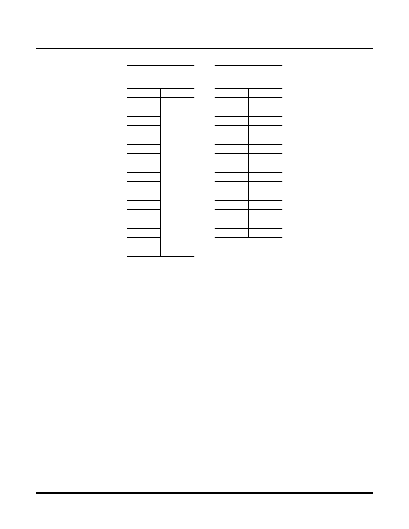
Table 3. Nominal Output Duty Cycle vs. V-Divider Setting
PLL_BYPASS Mode
The PLL_BYPASS mode is provided so that input reference signals can be coupled through to the outputs without
using the PLL functions. When PLL_BYPASS mode is enabled (PLL_BYPASS=HIGH), the output of the M divider
is routed directly to the inputs of the V dividers. In PLL_BYPASS mode, the nominal values of the V dividers are
halved, so that they provide division ratios ranging from 1 to 32. The output frequency for a given V divider (f
k
) will
be determined by
(2)
Please note that PLL_BYPASS mode is provided primarily for testing purposes. When PLL_BYPASS mode is
enabled, features such as lock detect and skew generation are unavailable.
Reference and External Feedback Inputs
The ispClock5600 provide sets of con
fi
gurable, internally-terminated inputs for both clock reference and feedback
signals. In normal operation, the one of the clock reference input pairs (REFA+/- or REFB+/-) is used as a clock
input.
The external feedback inputs make it possible to sample an output signal at the point of delivery. This makes it pos-
sible to provide output clocks which have very low skews in relation to the reference clock regardless of loading
effects.
The ispClock5610 provides one input signal pair for reference input and one input pair for external feedback, while
the ispClock5620 provides two pairs for reference signals and two pairs for feedback. To select between reference
and feedback inputs, the ispClock5620 provides two CMOS-compatible digital inputs called REFSEL and FBKSEL.
Table 4 shows the behavior of these two control inputs.
Divider Settings
with 50% Output
Duty Cycle
Divider Settings with
Non-50% Output Duty
Cycles
V
DC%
V
DC%
2
50
6
33
4
10
40
8
14
43
12
18
44
16
22
45
20
26
46
24
30
47
28
34
47
32
38
47
36
42
48
40
46
48
44
50
48
48
54
48
52
58
48
56
62
48
60
64
=
f
k
f
ref
x 2
M x V
k
相關(guān)PDF資料 |
PDF描述 |
|---|---|
| ISPPAC-CLK5620V-01TN48C | LED Area Light; LED Color:Red; Leaded Process Compatible:No; Light Emitting Area:62x62mm; Peak Reflow Compatible (260 C):No; Supply Current:200mA; Supply Voltage:24VDC; Wavelength:630nm |
| ISPPAC-CLK5610V-01TN48I | Backlight LED; Color:Red; Digit/Alpha Height:70mm; Forward Current:250mA; Operating Temperature Range:0 C to +50 C; Leaded Process Compatible:No; Light Emitting Area:70x70mm; Peak Reflow Compatible (260 C):No; Supply Current:250mA |
| ISPPAC-CLK5620V-01TN48I | Backlight LED; Color:Red; Digit/Alpha Height:85mm; Forward Current:500mA; Operating Temperature Range:0 C to +50 C; Leaded Process Compatible:No; Light Emitting Area:85x220mm; Peak Reflow Compatible (260 C):No |
| ISPPAC-POWR1014 | In-System Programmable Power Supply Supervisor, Reset Generator and Sequencing Controller |
| ISPPAC-POWR1014-01T48I | In-System Programmable Power Supply Supervisor, Reset Generator and Sequencing Controller |
相關(guān)代理商/技術(shù)參數(shù) |
參數(shù)描述 |
|---|---|
| ISPPAC-CLK5610V-01TN48I | 功能描述:時(shí)鐘驅(qū)動(dòng)器及分配 PROGRAMMABLE ZERO DELAY CL GEN RoHS:否 制造商:Micrel 乘法/除法因子:1:4 輸出類(lèi)型:Differential 最大輸出頻率:4.2 GHz 電源電壓-最大: 電源電壓-最小:5 V 最大工作溫度:+ 85 C 封裝 / 箱體:SOIC-8 封裝:Reel |
| ispPAC-CLK5620AV-01T100C | 功能描述:時(shí)鐘驅(qū)動(dòng)器及分配 ISP 0 Delay Clock Ge n w/Unv Fan-Out Buf RoHS:否 制造商:Micrel 乘法/除法因子:1:4 輸出類(lèi)型:Differential 最大輸出頻率:4.2 GHz 電源電壓-最大: 電源電壓-最小:5 V 最大工作溫度:+ 85 C 封裝 / 箱體:SOIC-8 封裝:Reel |
| ISPPACCLK5620AV-01T100C | 制造商:LATTICE 制造商全稱(chēng):Lattice Semiconductor 功能描述:In-System Programmable, Enhanced Zero-Delay, Clock Generator with Universal Fan-Out Buffer |
| ispPAC-CLK5620AV-01T100I | 功能描述:時(shí)鐘驅(qū)動(dòng)器及分配 ISP 0 Dlay Clck Gen w/Unv Fan-Out Buf I RoHS:否 制造商:Micrel 乘法/除法因子:1:4 輸出類(lèi)型:Differential 最大輸出頻率:4.2 GHz 電源電壓-最大: 電源電壓-最小:5 V 最大工作溫度:+ 85 C 封裝 / 箱體:SOIC-8 封裝:Reel |
| ISPPACCLK5620AV-01T100I | 制造商:LATTICE 制造商全稱(chēng):Lattice Semiconductor 功能描述:In-System Programmable, Enhanced Zero-Delay, Clock Generator with Universal Fan-Out Buffer |
發(fā)布緊急采購(gòu),3分鐘左右您將得到回復(fù)。