- 您現(xiàn)在的位置:買賣IC網(wǎng) > PDF目錄384535 > ISPGDXTMFAMILY (Lattice Semiconductor Corporation) JT 100C 100#22D PIN RECP PDF資料下載
參數(shù)資料
| 型號(hào): | ISPGDXTMFAMILY |
| 廠商: | Lattice Semiconductor Corporation |
| 元件分類: | TVS-瞬態(tài)抑制二極管 |
| 英文描述: | JT 100C 100#22D PIN RECP |
| 中文描述: | 在系統(tǒng)可編程通用數(shù)字CrosspointTM |
| 文件頁數(shù): | 8/25頁 |
| 文件大?。?/td> | 326K |
| 代理商: | ISPGDXTMFAMILY |
8
Specifications
ispGDX Family
External Timing Parameters
Over Recommended Operating Conditions
ns
ns
MHz
ns
ns
ns
ns
ns
ns
ns
ns
ns
ns
ns
ns
ns
ns
ns
ns
ns
–
–
111
4.0
4.0
0.0
–
–
–
–
–
–
–
3.5
3.5
–
10.0
–
–
5.0
6.5
–
–
–
–
5
8.5
6.0
9.5
6.0
6.0
9.0
9.0
–
–
14.0
–
5.0
0.5
–
–
80.0
5.5
5.5
0.0
–
–
–
–
–
–
–
5.0
5.0
–
14.0
–
–
7.0
9.0
–
–
–
–
7.0
11.0
9.0
13.0
8.5
8.5
12.0
12.0
–
–
18.0
–
7.0
0.5
1
2
3
4
5
6
7
8
9
10
11
12
13
14
15
16
17
18
19
20
A
A
–
–
–
–
A
A
A
A
B
C
B
C
–
–
–
–
A
A
Data Propagation Delay from any I/O pin to any I/O pin
Data Propagation Delay from MUXsel Inputs to any Output
Clock Frequency with External Feedback
Input Latch or Register Setup Time before any Clk
Output Latch or Register MUX Data Setup Time before any Clk
Latch or Register Hold Time after any Clk
Output Latch or Register Clk (from Y
x
) to Output Delay
Input Latch or Register Clk (from Y
x
) to Output Delay
Output Latch or Register Clk (from I/O pin) to Output Delay
Input Latch or Register Clock (from I/O pin) to Output Delay
Input to Output Enable
Input to Output Disable
Test OE Output Enable
Test OE Output Disable
Clock Pulse Duration, High
Clock Pulse Duration, Low
Register Reset Delay from RESET Low
Reset pulse width
Output Delay Adder for Output Timings Using Slow Slew Rate
Output Skew (tgco1 across chip)
1. All timings measured with one output switching, fast output slew rate setting, except
t
sl
.
t
pd
t
sel
f
max(ext)
t
su1
t
su2
t
h
t
gco1
t
gco2
t
co1
t
co2
t
en
t
dis
t
toeen
t
toedis
t
wh
t
wl
t
rst
t
rw
t
sl
t
sk
DESCRIPTION
PARAMETER
TEST
1
COND.
#
( )
1
UNITS
-5
MIN. MAX.
-7
MIN. MAX.
2
8
0
10
4
20
30
40
50
60
70
I/O Cell Fanout
6
10
4
Maximum
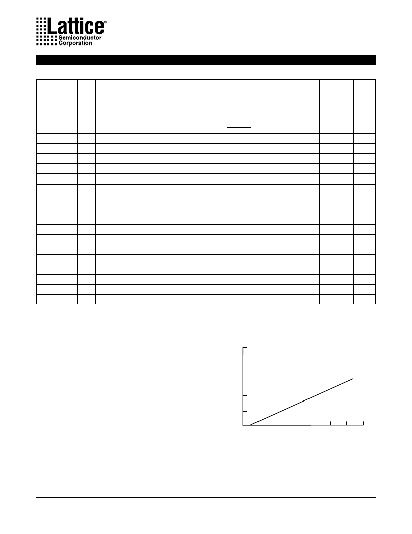
GRP Delay vs. I/O Cell Fanout
ispGDX timings are specified with a GRP load (fanout) of
four I/O cells. The figure at right shows the Maximum
GRP Delay with increased GRP loads. These deltas
apply to any signal path traversing the GRP (MUXA-D,
OE, CLK, MUXsel0-1). Global Clock signals, which do
not use the GRP, have no fanout delay adder.
相關(guān)PDF資料 |
PDF描述 |
|---|---|
| ISPGDX160A-5B272 | In-System Programmable Generic Digital CrosspointTM |
| ISPGDX80VA-7T100 | In-System Programmable 3.3V Generic Digital CrosspointTM |
| ISPGDX80VA-3T100 | In-System Programmable 3.3V Generic Digital CrosspointTM |
| ISPGDX80VA-5T100 | In-System Programmable 3.3V Generic Digital CrosspointTM |
| ISPGDX80VA-5T100I | In-System Programmable 3.3V Generic Digital CrosspointTM |
相關(guān)代理商/技術(shù)參數(shù) |
參數(shù)描述 |
|---|---|
| ISPHEADER01 | 制造商:Xeltek Inc 功能描述:ISP10/D10 |
| ISPICR1 | 功能描述:ADAPTER IN-CIRCUIT PROGRAMMING RoHS:否 類別:編程器,開發(fā)系統(tǒng) >> 配件 系列:- 產(chǎn)品培訓(xùn)模塊:Lead (SnPb) Finish for COTS Obsolescence Mitigation Program RoHS指令信息:IButton RoHS Compliance Plan 標(biāo)準(zhǔn)包裝:1 系列:- 附件類型:USB 至 1-Wire? RJ11 適配器 適用于相關(guān)產(chǎn)品:1-Wire? 設(shè)備 產(chǎn)品目錄頁面:1429 (CN2011-ZH PDF) |
| ISPL1048E-100LQ | 制造商:LATTICE 制造商全稱:Lattice Semiconductor 功能描述:High-Density Programmable Logic |
| ISPL1048E-100LQI | 制造商:LATTICE 制造商全稱:Lattice Semiconductor 功能描述:High-Density Programmable Logic |
| ISPL1048E-100LT | 制造商:LATTICE 制造商全稱:Lattice Semiconductor 功能描述:High-Density Programmable Logic |
發(fā)布緊急采購,3分鐘左右您將得到回復(fù)。