- 您現(xiàn)在的位置:買賣IC網(wǎng) > PDF目錄384535 > ISPGDXTMFAMILY (Lattice Semiconductor Corporation) JT 100C 100#22D PIN RECP PDF資料下載
參數(shù)資料
| 型號: | ISPGDXTMFAMILY |
| 廠商: | Lattice Semiconductor Corporation |
| 元件分類: | TVS-瞬態(tài)抑制二極管 |
| 英文描述: | JT 100C 100#22D PIN RECP |
| 中文描述: | 在系統(tǒng)可編程通用數(shù)字CrosspointTM |
| 文件頁數(shù): | 4/25頁 |
| 文件大?。?/td> | 326K |
| 代理商: | ISPGDXTMFAMILY |
4
Specifications
ispGDX Family
Applications
The ispGDX family architecture has been developed to
deliver an in-system programmable signal routing solu-
tion with high speed and high flexibility. The devices are
targeted for three similar but distinct classes of end-
system applications:
Programmable, Random Signal Interconnect (PRSI)
This class includes PCB-level programmable signal rout-
ing and may be used to provide arbitrary signal swapping
between chips. It opens up the possibilities of program-
mable system hardware. It is characterized by the need
to provide a large number of 1:1 pin connections which
are statically configured, i.e., the pin-to-pin paths do not
need to change dynamically in response to control in-
puts.
Programmable Data Path (PDP)
This application area includes system data path trans-
ceiver, MUX and latch functions. With today
’
s 32- and
64-bit microprocessor buses, but standard data path glue
components still relegated primarily to eight bits, PCBs
are frequently crammed with a dozen or more data path
glue chips that use valuable real estate. Many of these
applications consist of
“
on-board
”
bus and memory inter-
faces that do not require the very high drive of standard
glue functions but can benefit from higher integration.
Therefore, there is a need for a flexible means to inte-
grate these on-board data path functions in an analogous
way to programmable logic
’
s solution to control logic
integration. Lattice
’
s ispLSI High-Density PLDs make an
ideal control logic complement to the ispGDX in-system
programmable data path devices as shown below.
Programmable Switch Replacement (PSR)
Includes solid-state replacement and integration of me-
chanical DIP Switch and jumper functions. Through
in-system programming, pins of the ispGDX devices can
be driven to HIGH or LOW logic levels to emulate the
traditional device outputs. PSR functions do not require
any input pin connections.
These applications actually require somewhat different
silicon features. PRSI functions require that the device
support arbitrary signal routing on-chip between any two
pins with no routing restrictions. The routing connections
are static (determined at programming time) and each
input-to-output path operates independently. As a result,
there is little need for dynamic signal controls (OE,
clocks, etc.). Because the ispGDX device will interface
with control logic outputs from other components (such
as ispLSI) on the board (which frequently change late in
the design process as control logic is finalized), there
must be no restrictions on pin-to-pin signal routing for this
type of application.
PDP functions, on the other hand, require the ability to
dynamically switch signal routing (MUXing) as well as
latch and tri-state output signals. As a result, the pro-
grammable interconnect is used to define possible signal
routes that are then selected dynamically by control
signals from an external MPU or control logic. These
functions are usually formulated early in the conceptual
design of a product. The data path requirements are
driven by the microprocessor, bus and memory architec-
ture defined for the system. This part of the design is the
earliest portion of the system design frozen, and will not
usually change late in the design because the result
would be total system and PCB redesign. As a result, the
ability to accommodate arbitrary any pin-to-any pin re-
routing is not a strong requirement as long as the designer
has the ability to define his functions with a reasonable
degree of freedom initially.
As a result, the ispGDX architecture has been defined to
support PSR and PRSI applications (including bidirec-
tional paths) with no restrictions, while PDP applications
(using dynamic MUXing) are supported with a minimal
number of restrictions as described below. In this way,
speed and cost can be optimized and the devices can still
support the system designer
’
s needs.
The following diagrams illustrate several ispGDX appli-
cations.
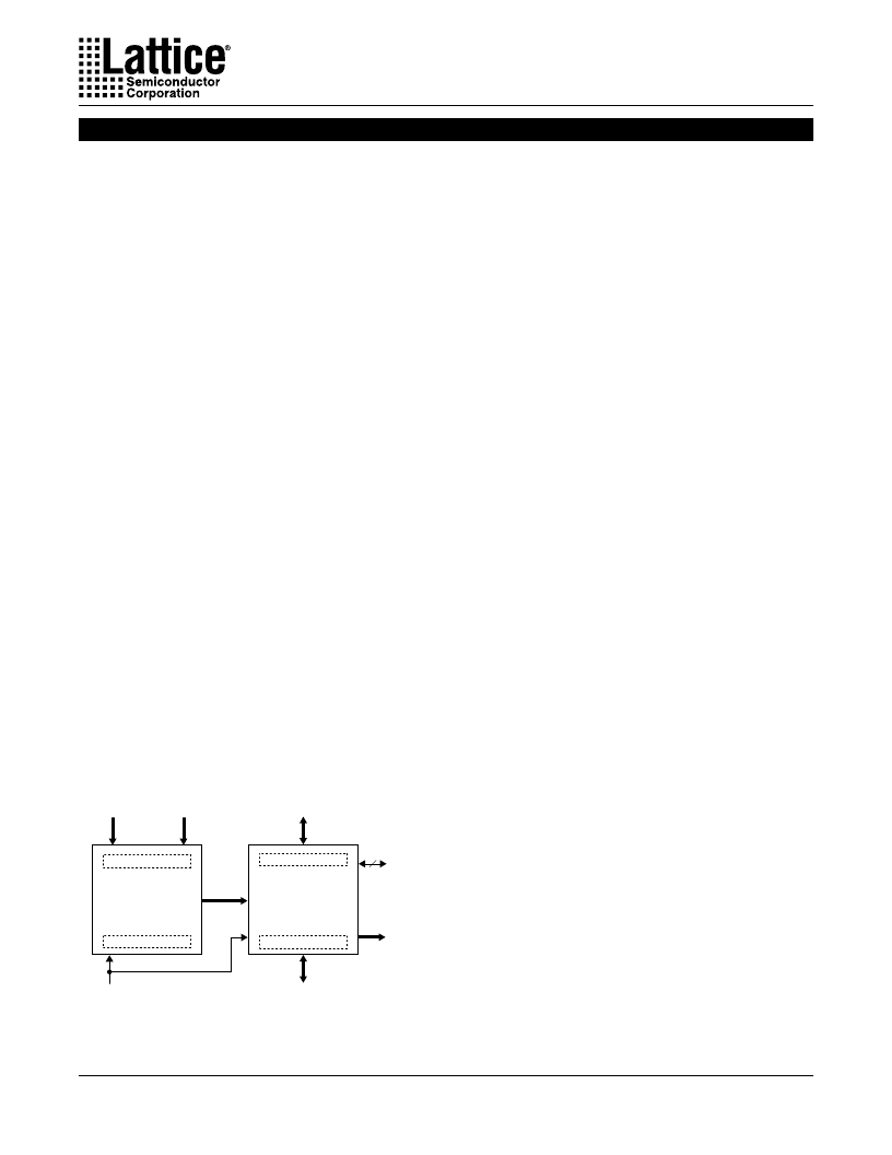
Data Path
Bus #1
Control
Inputs
(from
μ
P)
Address
Inputs
(from
μ
P)
Control
Outputs
System
Clock(s)
Data Path
Bus #2
Configuration
(Switch)
Outputs
ISP/JTAG
Interface
ispLSI Device
ispGDX Device
State Machines
Decoders
Buffers / Registers
Buffers / Registers
Figure 2. ispGDX Complements Lattice ispLSI
相關(guān)PDF資料 |
PDF描述 |
|---|---|
| ISPGDX160A-5B272 | In-System Programmable Generic Digital CrosspointTM |
| ISPGDX80VA-7T100 | In-System Programmable 3.3V Generic Digital CrosspointTM |
| ISPGDX80VA-3T100 | In-System Programmable 3.3V Generic Digital CrosspointTM |
| ISPGDX80VA-5T100 | In-System Programmable 3.3V Generic Digital CrosspointTM |
| ISPGDX80VA-5T100I | In-System Programmable 3.3V Generic Digital CrosspointTM |
相關(guān)代理商/技術(shù)參數(shù) |
參數(shù)描述 |
|---|---|
| ISPHEADER01 | 制造商:Xeltek Inc 功能描述:ISP10/D10 |
| ISPICR1 | 功能描述:ADAPTER IN-CIRCUIT PROGRAMMING RoHS:否 類別:編程器,開發(fā)系統(tǒng) >> 配件 系列:- 產(chǎn)品培訓(xùn)模塊:Lead (SnPb) Finish for COTS Obsolescence Mitigation Program RoHS指令信息:IButton RoHS Compliance Plan 標準包裝:1 系列:- 附件類型:USB 至 1-Wire? RJ11 適配器 適用于相關(guān)產(chǎn)品:1-Wire? 設(shè)備 產(chǎn)品目錄頁面:1429 (CN2011-ZH PDF) |
| ISPL1048E-100LQ | 制造商:LATTICE 制造商全稱:Lattice Semiconductor 功能描述:High-Density Programmable Logic |
| ISPL1048E-100LQI | 制造商:LATTICE 制造商全稱:Lattice Semiconductor 功能描述:High-Density Programmable Logic |
| ISPL1048E-100LT | 制造商:LATTICE 制造商全稱:Lattice Semiconductor 功能描述:High-Density Programmable Logic |
發(fā)布緊急采購,3分鐘左右您將得到回復(fù)。