- 您現(xiàn)在的位置:買賣IC網(wǎng) > PDF目錄370792 > HYB511000BJ-70 (SIEMENS A G) 1 M x 1-Bit Dynamic RAM Low Power 1 M ⅴ 1-Bit Dynamic RAM PDF資料下載
參數(shù)資料
| 型號: | HYB511000BJ-70 |
| 廠商: | SIEMENS A G |
| 元件分類: | DRAM |
| 英文描述: | 1 M x 1-Bit Dynamic RAM Low Power 1 M ⅴ 1-Bit Dynamic RAM |
| 中文描述: | 1M X 1 FAST PAGE DRAM, 70 ns, PDSO20 |
| 文件頁數(shù): | 5/22頁 |
| 文件大小: | 192K |
| 代理商: | HYB511000BJ-70 |
Semiconductor Group
37
HYB 511000BJ/BJL-50/-60/-70
1 M
×
1-DRAM
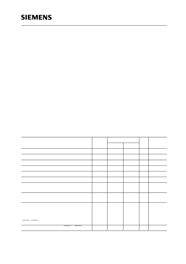
Absolute Maximum Ratings
Operating temperature range .........................................................................................0 to + 70 C
Storage temperature range......................................................................................– 55 to + 150 C
Soldering temperature ............................................................................................................260 C
Soldering time.............................................................................................................................10 s
Input/output voltage ........................................................................................................– 1 to + 7 V
Test Function Input voltage .......................................................................................– 1 to + 10.5 V
Power supply voltage......................................................................................................– 1 to + 7 V
Power dissipation.....................................................................................................................0.6 W
Data out current (short circuit) ................................................................................................50 mA
Note:
Stresses above those listed under “Absolute Maximum Ratings” may cause permanent
damage of the device. Exposure to absolute maximum rating conditions for extended periods
may affect device reliability.
DC Characteristics
T
A
= 0 to 70 C;
V
SS
= 0 V;
V
CC
= 5 V
±
10 %
Parameter
Symbol
Limit Values
Unit Test
Condition
min.
max.
Input high voltage
V
IH
V
IL
V
IH(TF)
V
IL(TF)
V
OH
V
OL
I
I(L)
2.4
6.5
V
1)
Input low voltage
– 1.0
V
CC
+ 4.5 10.5
– 1.0
0.8
V
1)
Test enable input high voltage
V
1)
Test disable input low voltage
Output high voltage (
I
OUT
= – 5 mA)
Output low voltage (
I
OUT
= 4.2 mA)
Input leakage current, any input except TF
(0 V
≤
V
IN
≤
6.5 V, all other pins = 0 V)
Output leakage current
(DO is disabled, 0 V
≤
V
OUT
≤
5.5 V)
Average
V
CC
supply current:
V
CC
+ 1.0 V
–
1)
2.4
V
1)
–
0.4
V
μ
A
1)
– 10
10
1)
I
O(L)
– 10
10
μ
A
1)
-50 version
-60 version
-70 version
(RAS, CAS, address cycling:
t
RC
=
t
RC
min.)
Standby
V
CC
supply current (RAS = CAS =
V
IH
)
I
CC2
I
CC1
–
–
–
90
80
70
mA
mA
mA
2) 3)
2) 3)
2) 3)
–
2
mA
–
相關PDF資料 |
PDF描述 |
|---|---|
| HYB511000BJL-50 | 1 M x 1-Bit Dynamic RAM Low Power 1 M ⅴ 1-Bit Dynamic RAM |
| HYB511000BJL-60 | 1 M x 1-Bit Dynamic RAM Low Power 1 M ⅴ 1-Bit Dynamic RAM |
| HYB511000BJ- | 1 M x 1-Bit Dynamic RAM Low Power 1 M ⅴ 1-Bit Dynamic RAM |
| HYB511000BJL-70 | 1 M x 1-Bit Dynamic RAM Low Power 1 M ⅴ 1-Bit Dynamic RAM |
| HYB5116400BJ-50 | 4M x 4-Bit Dynamic RAM |
相關代理商/技術參數(shù) |
參數(shù)描述 |
|---|---|
| HYB511000BJ-80 | 制造商:未知廠家 制造商全稱:未知廠家 功能描述:x1 Fast Page Mode DRAM |
| HYB511000BJL-50 | 制造商:INFINEON 制造商全稱:Infineon Technologies AG 功能描述:1 M x 1-Bit Dynamic RAM Low Power 1 M ⅴ 1-Bit Dynamic RAM |
| HYB511000BJL-60 | 制造商:INFINEON 制造商全稱:Infineon Technologies AG 功能描述:1 M x 1-Bit Dynamic RAM Low Power 1 M ⅴ 1-Bit Dynamic RAM |
| HYB511000BJL-70 | 制造商:INFINEON 制造商全稱:Infineon Technologies AG 功能描述:1 M x 1-Bit Dynamic RAM Low Power 1 M ⅴ 1-Bit Dynamic RAM |
| HYB511000BL-60 | 制造商:未知廠家 制造商全稱:未知廠家 功能描述:x1 Fast Page Mode DRAM |
發(fā)布緊急采購,3分鐘左右您將得到回復。