- 您現(xiàn)在的位置:買賣IC網(wǎng) > PDF目錄370782 > HYB18T256324F-16 (INFINEON TECHNOLOGIES AG) 256-Mbit GDDR3 DRAM [600MHz] PDF資料下載
參數(shù)資料
| 型號: | HYB18T256324F-16 |
| 廠商: | INFINEON TECHNOLOGIES AG |
| 英文描述: | 256-Mbit GDDR3 DRAM [600MHz] |
| 中文描述: | 256兆GDDR3顯示內(nèi)存[600MHz的] |
| 文件頁數(shù): | 75/80頁 |
| 文件大?。?/td> | 2026K |
| 代理商: | HYB18T256324F-16 |
第1頁第2頁第3頁第4頁第5頁第6頁第7頁第8頁第9頁第10頁第11頁第12頁第13頁第14頁第15頁第16頁第17頁第18頁第19頁第20頁第21頁第22頁第23頁第24頁第25頁第26頁第27頁第28頁第29頁第30頁第31頁第32頁第33頁第34頁第35頁第36頁第37頁第38頁第39頁第40頁第41頁第42頁第43頁第44頁第45頁第46頁第47頁第48頁第49頁第50頁第51頁第52頁第53頁第54頁第55頁第56頁第57頁第58頁第59頁第60頁第61頁第62頁第63頁第64頁第65頁第66頁第67頁第68頁第69頁第70頁第71頁第72頁第73頁第74頁當(dāng)前第75頁第76頁第77頁第78頁第79頁第80頁
0.85
—
HYB18T256324F–[16/20/22]
256-Mbit DDR SGRAM
Electrical Characteristics
Data Sheet
75
Rev. 1.11, 04-2005
10292004-DOXT-FS0U
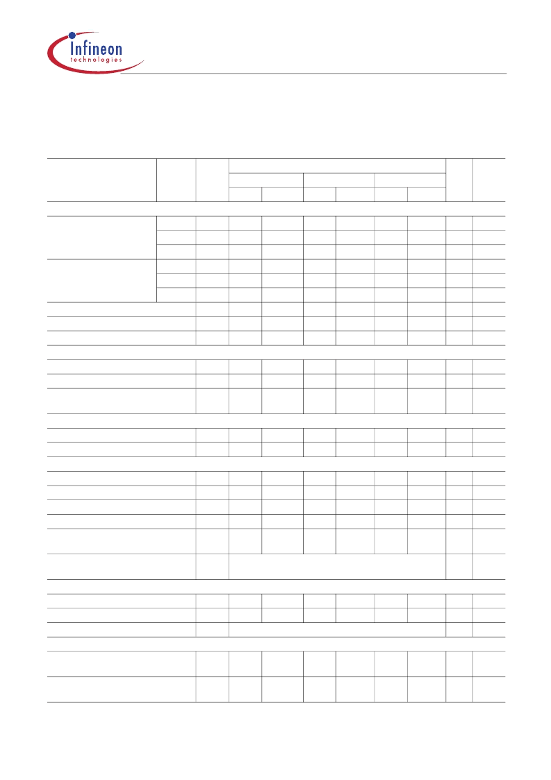
4.13
Summary of timing parameters for –1.6, –2.0 and –2.2 ns speed sorts in DLL
on mode
Table 43
Parameter
Timing Parameters for –1.6, –2.0 and –2.2 speed sorts
Read
latency
bol
Sym-
Limit Values
–1.6
min
Unit
Notes
–2.0
max
–2.2
max
max
min
min
Clock and Clock Enable
Clock Cycle Time
7
6
5
7
6
5
t
CK7
t
CK6
t
CK5
f
CK7
f
CK6
f
CK5
t
CH
t
CL
t
HP
1.6
2.0
—
300
300
—
0.45
0.45
0.45
3.3
3.3
—
600
500
—
0.55
0.55
—
2.0
2.0
—
250
250
—
0.45
0.45
0.45
4.0
4.0
—
500
500
—
0.55
0.55
—
2.2
2.2
2.7
250
250
250
0.45
0.45
0.45
4.0
4.0
4.0
455
455
370
0.55
0.55
—
ns
ns
ns
MHz
MHz
MHz
t
CK
t
CK
t
CK
System frequency
Clock high level width
Clock low-level width
Minimum clock half period
Command and Address Setup and Hold Timing
Address/Command input setup time
t
IS
Address/Command input hold time
Address/Command input pulse
width
Mode Register Set Timing
Mode Register Set cycle time
Mode Register Set to READ timing
t
MRDR
Row Timing
Row Cycle Time
Row Active Time
ACT(a) to ACT(b) Command period
t
RRD
Row Precharge Time
Row to Column Delay Time for
Reads
Row to Column Delay Time for
Writes
Column Timing
CAS(a) to CAS(b) Command period
t
CCD
Write to Read Command Delay
Read to Write command delay
Write Cycle Timing Parameters for Data and Data Strobe
Write command to first WDQS
latching transition
Data-in and Data Mask to WDQS
Setup Time
1)
0.6
0.6
—
—
0.75
0.75
0.85
—
—
—
0.75
0.75
0.85
—
—
—
ns
ns
t
CK
t
IH
t
IPW
t
MRD
5
15
—
—
4
12
—
—
4
12
—
—
t
CK
t
CK
t
RC
t
RAS
37.2
24.0
8.0
13.2
—
8 x t
REFI
—
—
—
37.2
24.0
8.0
13.2
16.0
—
8 x t
REFI
26.2
—
–
–
39.6
—
8 x t
REFI
ns
—
–
–
ns
8.8
13.2
17.5
ns
ns
ns
t
RP
t
RCDRD
16.0
t
RCDWR
t
RCDWR(min)
=
t
RCDRD(min)
- (WL + 1) x
t
CK(min)
ns
2
6.0
—
—
2
6.0
—
—
2
6.6
—
—
t
CK
ns
t
CK
2)
t
WTR
t
RTW
3)
t
RTW
(min)= (CL+4-WL)
4)
t
DQSS
WL -
0.25
0.35
WL
+0.25
—
WL -
0.25
0.375
WL
+0.25
—
WL -
0.25
0.375
WL
+0.25
—
t
CK
t
DS
ns
相關(guān)PDF資料 |
PDF描述 |
|---|---|
| HYB18T256324F-20 | 256-Mbit GDDR3 DRAM [600MHz] |
| HYB18T256324F-22 | 256-Mbit GDDR3 DRAM [600MHz] |
| HYB18T256400AFL-3 | 256 Mbi t DDR2 SDRAM |
| HYB18T256160A-3S | 256 Mbi t DDR2 SDRAM |
| HYB18T256800AFL-3 | 256 Mbi t DDR2 SDRAM |
相關(guān)代理商/技術(shù)參數(shù) |
參數(shù)描述 |
|---|---|
| HYB18T256400AF-3.7 | 制造商:Infineon Technologies AG 功能描述:64M X 4 DDR DRAM, 0.5 ns, PBGA60 |
| HYB18T256400AF-5 | 制造商:Infineon Technologies AG 功能描述:SDRAM, DDR, 64M x 4, 60 Pin, Plastic, BGA |
| HYB18T256800AF-5 | 制造商:Infineon Technologies AG 功能描述: |
| HYB18T512161BF-25 | 制造商:Qimonda 功能描述:SDRAM, DDR, 32M x 16, 84 Pin, Plastic, BGA |
| HYB18T512400AF-5 | 制造商:Intersil Corporation 功能描述:SDRAM, DDR, 128M x 4, 60 Pin, Plastic, BGA |
發(fā)布緊急采購,3分鐘左右您將得到回復(fù)。