- 您現(xiàn)在的位置:買賣IC網(wǎng) > PDF目錄370740 > HY5PS12823LF 64Mx8|1.8V|8K|D43/D44/D54/D55|DDR II SDRAM - 512M PDF資料下載
參數(shù)資料
| 型號(hào): | HY5PS12823LF |
| 英文描述: | 64Mx8|1.8V|8K|D43/D44/D54/D55|DDR II SDRAM - 512M |
| 中文描述: | 64Mx8 | 1.8 | 8K的| D43/D44/D54/D55 |的DDR II內(nèi)存- 512M |
| 文件頁(yè)數(shù): | 57/66頁(yè) |
| 文件大?。?/td> | 862K |
| 代理商: | HY5PS12823LF |
第1頁(yè)第2頁(yè)第3頁(yè)第4頁(yè)第5頁(yè)第6頁(yè)第7頁(yè)第8頁(yè)第9頁(yè)第10頁(yè)第11頁(yè)第12頁(yè)第13頁(yè)第14頁(yè)第15頁(yè)第16頁(yè)第17頁(yè)第18頁(yè)第19頁(yè)第20頁(yè)第21頁(yè)第22頁(yè)第23頁(yè)第24頁(yè)第25頁(yè)第26頁(yè)第27頁(yè)第28頁(yè)第29頁(yè)第30頁(yè)第31頁(yè)第32頁(yè)第33頁(yè)第34頁(yè)第35頁(yè)第36頁(yè)第37頁(yè)第38頁(yè)第39頁(yè)第40頁(yè)第41頁(yè)第42頁(yè)第43頁(yè)第44頁(yè)第45頁(yè)第46頁(yè)第47頁(yè)第48頁(yè)第49頁(yè)第50頁(yè)第51頁(yè)第52頁(yè)第53頁(yè)第54頁(yè)第55頁(yè)第56頁(yè)當(dāng)前第57頁(yè)第58頁(yè)第59頁(yè)第60頁(yè)第61頁(yè)第62頁(yè)第63頁(yè)第64頁(yè)第65頁(yè)第66頁(yè)
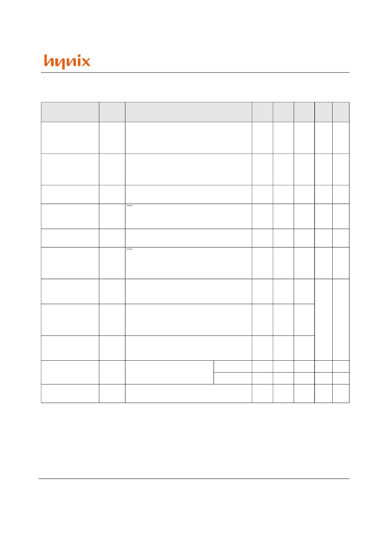
Rev. 0.52/Nov. 02 57
HY5PS12423(L)F
HY5PS12823(L)F
HY5PS121623(L)F
DC CHARACTERISTICS II
(TA=0 to 70
o
C, Voltage referenced to V
SS
= 0V)
Parameter
Symbol
Test Condition
533
4/4/4
400
3/3/3
4/4/4Unit Note
Operating Current
IDD0
One ban; Active - Precharge; tRC=tRC(min);
tCK=tCK(min); DQ,DM and DQS inputs changing
twice per clock cycle; address and control inputs
changing once per clock cycle
TBD
TBD
TBD
mA
Operating Current
I
DD1
One bank; Active - Read - Precharge;
Burst Length=4; tRC=tRC(min); tCK=tCK(min);
address and control inputs changing once per clock
cycle
TBD
TBD
TBD
mA
Precharge Power Down
Standby Current
I
DD2P
All banks idle; Power down mode; CKE=Low,
tCK=tCK(min)
TBD
TBD
TBD
mA
Idle Standby Current
I
DD2F
CS=High, All banks idle; tCK=tCK(min);
CKE=High; address and control inputs changing once
per clock cycle. VIN = VREF for DQ, DQS and DM
TBD
TBD
TBD
mA
Active Power Down
Standby Current
I
DD3P
One bank active; Power down mode; CKE=Low,
tCK=tCK(min)
TBD
TBD
TBD
mA
Active Standby Current
I
DD3N
CS=HIGH; CKE=HIGH; One bank; Active-Precharge;
tRC=tRAS(max); tCK=tCK(min); DQ, DM and DQS
inputs changing twice per clock cycle; Address and
other control inputs changing once per clock cycle
TBD
TBD
TBD
mA
Operating Current
I
DD4R
Burst=4; Reads; Continuous burst; One bank active;
Address and control inputs changing once per clock
cycle; tCK=tCK(min); IOUT=0mA
TBD
TBD
TBD
mA
Operating Current
I
DD4W
Burst=4; Writes; Continuous burst; One bank active;
Address and control inputs changing once per clock
cycle; tCK=tCK(min); DQ, DM and DQS inputs
changing twice per clock cycle
TBD
TBD
TBD
Auto Refresh Current
I
DD5
tRC=tRFC(min) - 8*tCK for DDR200 at 100Mhz,
10*tCK for DDR266A & DDR II at 133Mhz; distributed
refresh
TBD
TBD
TBD
Self Refresh Current
I
DD6
CKE =< 0.2V; External clock on;
tCK=tCK(min)
Normal
TBD
TBD
TBD
mA
Low Power
TBD
TBD
TBD
mA
Operating Current -
Four Bank Operation
I
DD7
Four bank interleaving with BL=4, Refer to the
following page for detailed test condition
TBD
TBD
TBD
mA
This Page will be changed by the standardization result of Jedec Committee.
相關(guān)PDF資料 |
PDF描述 |
|---|---|
| HY5P | Current Transducers HY 5 to 25-P/SP1 |
| HY5R256HC | -|2.5V|8K|40|Direct RDRAM - 256M |
| HY5R288HC | -|2.5V|8K|40|Direct RDRAM - 288M |
| HY5V16CF | 1Mx16|3.3V|4K|H|SDR SDRAM - 16M |
| HY5V16CF-H | x16 SDRAM |
相關(guān)代理商/技術(shù)參數(shù) |
參數(shù)描述 |
|---|---|
| HY5PS1G1631AFP | 制造商:HYNIX 制造商全稱:Hynix Semiconductor 功能描述:1Gb DDR2 SDRAM |
| HY5PS1G1631AFP-Y5 | 制造商:HYNIX 制造商全稱:Hynix Semiconductor 功能描述:1Gb DDR2 SDRAM |
| HY5PS1G1631ALFP | 制造商:HYNIX 制造商全稱:Hynix Semiconductor 功能描述:1Gb DDR2 SDRAM |
| HY5PS1G1631ALFP-Y5 | 制造商:HYNIX 制造商全稱:Hynix Semiconductor 功能描述:1Gb DDR2 SDRAM |
| HY5PS1G1631CFP | 制造商:HYNIX 制造商全稱:Hynix Semiconductor 功能描述:1Gb DDR2 SDRAM |
發(fā)布緊急采購(gòu),3分鐘左右您將得到回復(fù)。