- 您現(xiàn)在的位置:買賣IC網(wǎng) > PDF目錄385403 > HT82J97E-20SOP-A (Holtek Semiconductor Inc.) USB Joystick Encoder 8-Bit OTP MCU PDF資料下載
參數(shù)資料
| 型號(hào): | HT82J97E-20SOP-A |
| 廠商: | Holtek Semiconductor Inc. |
| 英文描述: | USB Joystick Encoder 8-Bit OTP MCU |
| 中文描述: | USB搖桿編碼器8位微控制器檢察官辦公室 |
| 文件頁數(shù): | 6/46頁 |
| 文件大?。?/td> | 314K |
| 代理商: | HT82J97E-20SOP-A |
第1頁第2頁第3頁第4頁第5頁當(dāng)前第6頁第7頁第8頁第9頁第10頁第11頁第12頁第13頁第14頁第15頁第16頁第17頁第18頁第19頁第20頁第21頁第22頁第23頁第24頁第25頁第26頁第27頁第28頁第29頁第30頁第31頁第32頁第33頁第34頁第35頁第36頁第37頁第38頁第39頁第40頁第41頁第42頁第43頁第44頁第45頁第46頁

HT82J97E
Rev. 1.30
6
May 10, 2004
Stack Register
STACK
This is a special part of the memory which is used to
save the contents of the program counter (PC) only. The
stack is organized into 8 levels and is neither part of the
data nor part of the program space, and is neither read-
able nor writeable. The activated level is indexed by the
stack pointer (SP) and is neither readable nor writeable.
At a subroutine call or interrupt acknowledge signal, the
contents of the program counter are pushed onto the
stack. At the end of a subroutine or an interrupt routine,
signaled by a return instruction (RET or RETI), the pro-
gram counter is restored to its previous value from the
stack.Afterachipreset,theSPwillpointtothetopofthe
stack.
If the stack is full and a non-masked interrupt takes
place, the interrupt request flag will be recorded but the
acknowledge signal will be inhibited. When the stack
pointer is decremented (by RET or RETI), the interrupt
will be serviced. This feature prevents stack overflow al-
lowing the programmer to use the structure more easily.
In a similar case, if the stack is full and a CALL is sub-
sequently executed, stack overflow occurs and the first
entry will be lost (only the most recent 8 return ad-
dresses are stored).
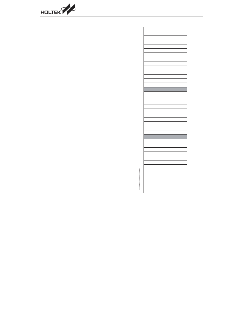
Data Memory
RAM for Bank 0
The data memory is designed with 96 8 bits. The data
memory is divided into two functional groups: special
function registers and general purpose data memory
(96 8). Most are read/write, but some are read only.
The special function registers include the indirect ad-
dressing registers (R0;00H, R1;02H), Bank register (BP,
04H), PWM1 duty register (0DH), PWM2 duty regis-
ter(0EH), Timer/Event Counter higher order byte regis-
ter (TMRH;0FH), Timer/Event Counter lower order byte
register (TMRL;10H), Timer/Event Counter control reg-
ister (TMRC;11H), program counter lower-order byte
register (PCL;06H), memory pointer registers
(MP0;01H, MP1;03H), accumulator (ACC;05H), table
pointers (TBLP;07H, TBHP;1FH), table higher-order
byte
register
(TBLH;08H),
(STATUS;0AH), interrupt control register (INTC;0BH),
Watchdog Timer option setting register (WDTS;09H),
I/O registers (PA;12H, PB;14H, PC;16H), PWM Base
Period Register (18H), I/O control registers (PAC;13H,
PBC;15H, PCC;17H). USB/PS2 status and control reg-
ister (USC;1AH), USB endpoint interrupt status register
(USR;1BH), system clock control register (SCC;1CH).
A/D converter status and control register (ADSC;1DH)
and A/D converter result register (ADR;1EH). The re-
maining space before the 20H is reserved for future ex-
status
register
panded usage and reading these locations will get
00H . The general purpose data memory, addressed
from 20H to 7FH, is used for data and control informa-
tion under instruction commands.
All of the data memory areas can handle arithmetic,
logic, increment, decrement and rotate operations di-
rectly. Except for some dedicated bits, each bit in the
data memory can be set and reset by SET [m].i and
CLR [m].i . They are also indirectly accessible through
memory pointer registers (MP0 or MP1).
2
2
2
7 2
* 2
/ 2
0 2
1 2
9 2
8 2
2
- 2
2
2
2
: 2
2
2
2
7 2
* 2
/ 2
0 2
1 2
9 2
&
, (
!
(
'
; 8 0 ( -
! <
2
- 2
2
2
2
: 2
1 : 2
2
"
(
" "
! !
(
!
(
"
(
" "
! !
(
!
(
-
#
- #
- # 2
+
+
(
(
!
+
(
(
!
2
#
-
-
+
( -
!
(
" (
!
( ;
<
- 2
-
> (
8 2
Bank 0 RAM Mapping
相關(guān)PDF資料 |
PDF描述 |
|---|---|
| HT82J97E-28SOP-A | USB Joystick Encoder 8-Bit OTP MCU |
| HT82K28 | Win98 Keyboard Encoder |
| HT82K28A | Win98 Keyboard Encoder |
| HT82K628A | Windows 2000 Keyboard Encoder(Windows 2000操作系統(tǒng)鍵盤編碼器) |
| HT82K628 | Windows 2000 Keyboard Encoder |
相關(guān)代理商/技術(shù)參數(shù) |
參數(shù)描述 |
|---|---|
| HT82J97E-28SOP-A | 制造商:HOLTEK 制造商全稱:Holtek Semiconductor Inc 功能描述:USB Joystick Encoder 8-Bit OTP MCU |
| HT82K19 | 制造商:未知廠家 制造商全稱:未知廠家 功能描述:Peripheral IC |
| HT82K28 | 制造商:HOLTEK 制造商全稱:Holtek Semiconductor Inc 功能描述:Win98 Keyboard Encoder |
| HT82K28A | 制造商:HOLTEK 制造商全稱:Holtek Semiconductor Inc 功能描述:Win98 Keyboard Encoder |
| HT82K28A_02 | 制造商:HOLTEK 制造商全稱:Holtek Semiconductor Inc 功能描述:Win98 Keyboard Encoder |
發(fā)布緊急采購,3分鐘左右您將得到回復(fù)。