- 您現(xiàn)在的位置:買(mǎi)賣(mài)IC網(wǎng) > PDF目錄385398 > HT27LC512 (Holtek Semiconductor Inc.) OTP CMOS 64Kx 8-Bit EPROM PDF資料下載
參數(shù)資料
| 型號(hào): | HT27LC512 |
| 廠商: | Holtek Semiconductor Inc. |
| 英文描述: | OTP CMOS 64Kx 8-Bit EPROM |
| 中文描述: | 檢察官辦公室的CMOS 64Kx 8位存儲(chǔ)器 |
| 文件頁(yè)數(shù): | 2/10頁(yè) |
| 文件大?。?/td> | 258K |
| 代理商: | HT27LC512 |
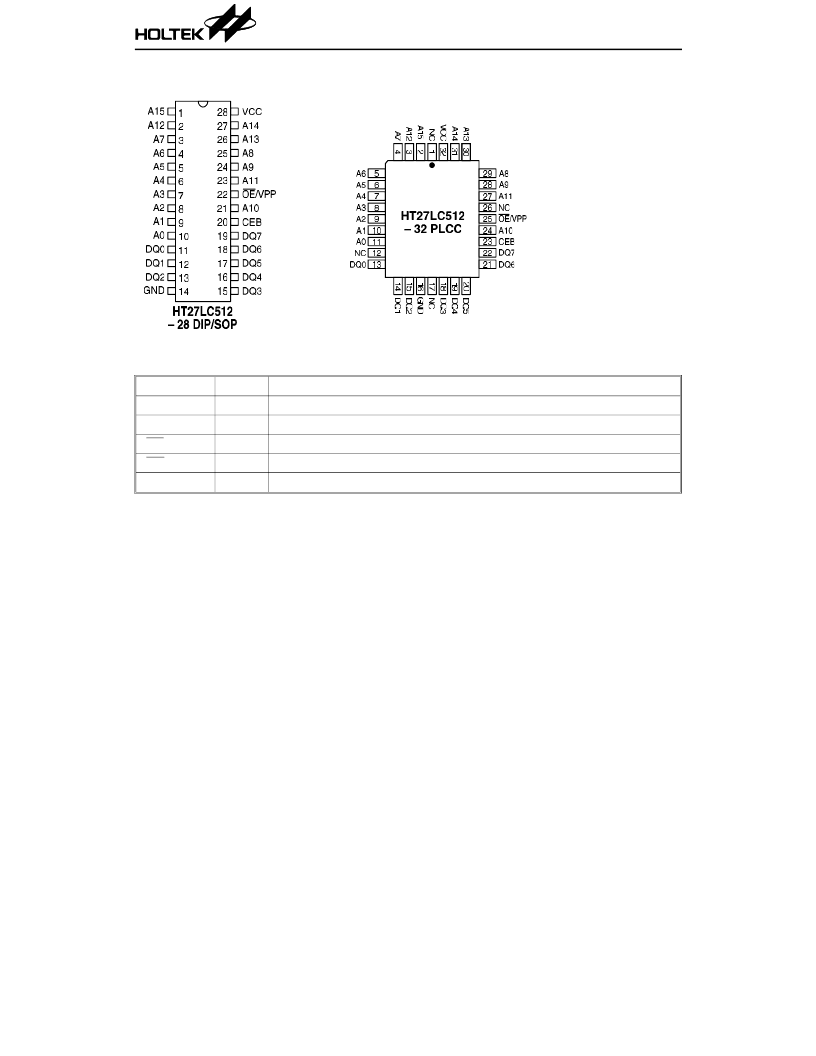
Pin Assignment
Pin Description
Pin Name
A0~A15
DQ0~DQ7
CE
OE /VPP
NC
I/O/C/P
I
I/O
C
C/P
—
Description
Address inputs
Data inputs/outputs
Chip enable
Output enable/program voltage supply
No connection
Absolute Maximum Ratings
Operation Temperature Commercial ...................................................................................0
°
C to +70
°
C
Storage Temperature.........................................................................................................–65
°
C to 125
°
C
Applied VCC Voltage with Respect to GND....................................................................... –0.6V to 7.0V
Applied Voltage on Input Pin with Respect to GND ......................................................... –0.6V to 7.0V
Applied Voltage on Output Pin with Respect to GND ............................................. –0.6V to V
CC
+0.5V
Applied Voltage on A9 Pin with Respect to GND ............................................................ –0.6V to 13.5V
Applied VPP Voltage with Respect to GND ......................................................................–0.6V to 13.5V
Applied READ Voltage (Functionality is guaranteed between these limits) ................... +3V to +3.6V
Note: These are stress ratings only. Stresses exceeding the range specified under “Absolute Maxi-
mum Ratings” may cause substantial damage to the device. Functional operation of this device
at other conditions beyond those listed in the specification is not implied and prolonged
exposure to extreme conditions may affect device reliability.
HT27LC512
2
6th May ’99
相關(guān)PDF資料 |
PDF描述 |
|---|---|
| HT2812 | Single Sound Generator |
| HT2812-14DIP | Single Sound Generator |
| HT2812-8DIP | Single Sound Generator |
| HT2812A | Single Sound Generator |
| HT2812B | Single Sound Generator |
相關(guān)代理商/技術(shù)參數(shù) |
參數(shù)描述 |
|---|---|
| HT27LC512(28DIP) | 制造商:未知廠家 制造商全稱(chēng):未知廠家 功能描述:x8 EPROM |
| HT27LC512(28SOP) | 制造商:未知廠家 制造商全稱(chēng):未知廠家 功能描述:x8 EPROM |
| HT27LC512(32PLCC) | 制造商:未知廠家 制造商全稱(chēng):未知廠家 功能描述:x8 EPROM |
| HT2801UL | 制造商:HYES 制造商全稱(chēng):HYES 功能描述:LCD MODULE (240 × RGB × 320) |
| HT2812 | 制造商:HOLTEK 制造商全稱(chēng):Holtek Semiconductor Inc 功能描述:Single Sound Generator |
發(fā)布緊急采購(gòu),3分鐘左右您將得到回復(fù)。