- 您現(xiàn)在的位置:買賣IC網(wǎng) > PDF目錄384442 > HS1-81C56RH (HARRIS SEMICONDUCTOR) Radiation Hardened 256 x 8 CMOS RAM PDF資料下載
參數(shù)資料
| 型號: | HS1-81C56RH |
| 廠商: | HARRIS SEMICONDUCTOR |
| 元件分類: | DRAM |
| 英文描述: | Radiation Hardened 256 x 8 CMOS RAM |
| 中文描述: | 256 X 8 MULTI-PORT SRAM, 250 ns, CDIP40 |
| 文件頁數(shù): | 11/14頁 |
| 文件大小: | 86K |
| 代理商: | HS1-81C56RH |
11
HS-81C55RH, HS-81C56RH
Input/Output Section
The I/O section of the HS-81C55RH and HS-81C56RH
consists of five registers: (See Figure 5)
Command/Status Register (C/S)
- Both register are
assigned the address XXXXX000. The C/S address
serves the dual prupose.
When the C/S registers are selected during WRITE
operation, a command is written into the command
register. The contents of this register are not accessible
through the pins.
When the C/S (XXXXX000) is selected during a READ
operation, the status information of the I/O ports and the
timer becomes available on the AD0 - AD7 lines.
PA Register
- This register can be programmed to be
either input or output ports depending on the status of the
contents of the C/S Register. also depending on the
command, this port can operate in either the basic mode
or the strobed mode (See timing diagram). the I/O pins
assigned in relation to this register are PA0 - PA7. The
address of this register is XXXXX001.
PB Register -
This register functions the same as PA
Register. the I/O pins assigned are PB0 - PB7. The
address of this register is XXXXX010
PC Register -
This register has the address XXXXX011
and contains only 6 bits. The 6 bits can be programmed to
be either input ports, output ports or as control signals for
PA and PB by properly programming the AD2 and AD3
bits of the C/S register.
When PC0 - PC5 is used as a control port, 3 bits are
assigned for Port A and 3 for Port B. The first bit is an
Interrupt that the HS-81C55RH and HS-81C56RH sends
out. The second is an output signal indicating whether the
buffer is full or empty, and the third is an input pin to
accept a strobe for the strobed input mode. (See Table 1).
When the ‘C’ port is programmed to either ALT3 or ALT4, the
control signals for PA and Pb are initialized as follows:
:
FIGURE 5. I/O PORT AND TIMER ADDRESSING SCHEME
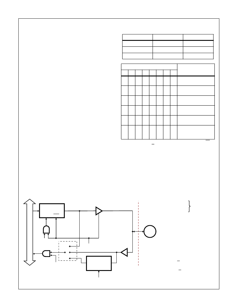
Figure 6 shows how I/O Ports A and B are structured within
the HS-81C55RH and HS-81C56RH.
Note in the diagram that when the I/O ports are programmed
to be output ports, the contents of the output ports can still
be read by a READ operation when appropriately
addressed.
CONTROL
INPUT MODE
OUTPUT MODE
BF
Low
Low
INTR
Low
High
STB
Input Control
Input Control
I/O ADDRESS
SELECTION
A7
A6
A5
A4
A3
A2
A1
A0
X
X
X
X
X
0
0
0
Interval Command/
Status Register
X
X
X
X
X
0
0
1
General Purpose I/O
Port A
X
X
X
X
X
0
1
0
General Purpose I/O
Port B
X
X
X
X
X
0
1
1
General Purpose I/O or
Control Port C
X
X
X
X
X
1
0
0
Low-Order 8 Bits of
Timer Count
X
X
X
X
X
1
0
1
High 6 Bits of Timer
Count and 2 Bits of Timer
Mode
I/O Address must be qualified by CE = 1(81C56RH) or CE =
0(81C55RH) and IO/M = 1 in order to select the appropriate register.
X = Don’t Care
FIGURE 6. HS-81C55RH AND HS-81C56RH PORT FUNCTION
OUTPUT
LATCH
D
Q
CLK
CLR
D
Q
LATCH
CLK
STB
(1)
(2)
(3)
READ
PORT
MODE (4)
WRITE
PORT
PA/PB
PIN
I
MUX
HS-81C55RH AND HS-81C56RH
ONE BIT OF PORT A OR PORT B
(1) OUTPUT MODE
(2) SIMPLE INPUT
(3) STROBED INPUT
(4) = 1 FOR OUTPUT MODE
= 0 FOR INPUT MODE
MULTIPLEXER
CONTROL
NOTES:
1. READ Port = (IO/M = 1)(RD = 0)(CE Active)
(Port Address Selected)
2. WRITE Port = (IO/M = 1)(wr = 0)(CE Active)
(Port Address Selected)
Spec Number
518056
相關(guān)PDF資料 |
PDF描述 |
|---|---|
| HS-81C55RH | Radiation Hardened 256 x 8 CMOS RAM |
| HS-81C56RH | Radiation Hardened 256 x 8 CMOS RAM |
| HS9-81C55RH | Radiation Hardened 256 x 8 CMOS RAM |
| HS9-81C56RH | Radiation Hardened 256 x 8 CMOS RAM |
| HS1-82C08RH-8 | Radiation Hardened 8-Bit Bus Transceiver |
相關(guān)代理商/技術(shù)參數(shù) |
參數(shù)描述 |
|---|---|
| HS1-81C56RH-8 | 制造商:INTERSIL 制造商全稱:Intersil Corporation 功能描述:Radiation Hardened 256 x 8 CMOS RAM |
| HS1-81C56RH-Q | 制造商:INTERSIL 制造商全稱:Intersil Corporation 功能描述:Radiation Hardened 256 x 8 CMOS RAM |
| HS1820A | 制造商:未知廠家 制造商全稱:未知廠家 功能描述:Peripheral IC |
| HS1820B | 制造商:未知廠家 制造商全稱:未知廠家 功能描述:Peripheral IC |
| HS18230 | 功能描述:SCHOTTKY RECTIFIER 180A 30V RoHS:是 類別:半導(dǎo)體模塊 >> 二極管,整流器 系列:- 標(biāo)準(zhǔn)包裝:10 系列:- 電壓 - 在 If 時為正向 (Vf)(最大):1.45V @ 30A 電流 - 在 Vr 時反向漏電:15µA @ 400V 電流 - 平均整流 (Io)(每個二極管):30A 電壓 - (Vr)(最大):400V 反向恢復(fù)時間(trr):65ns 二極管類型:標(biāo)準(zhǔn) 速度:快速恢復(fù) = 200mA(Io) 二極管配置:2 個獨立式 安裝類型:底座安裝 封裝/外殼:ISOTOP 供應(yīng)商設(shè)備封裝:ISOTOP? 包裝:管件 |
發(fā)布緊急采購,3分鐘左右您將得到回復(fù)。