- 您現(xiàn)在的位置:買賣IC網(wǎng) > PDF目錄370451 > HCPL-316J 2.0 Amp Gate Drive Optocoupler with Integrated (V CE ) Desaturation Detection and Fault Status Feedback(帶集成不飽和檢測(cè)和誤差反饋的2.0 Amp門驅(qū)動(dòng)耦合器) PDF資料下載
參數(shù)資料
| 型號(hào): | HCPL-316J |
| 英文描述: | 2.0 Amp Gate Drive Optocoupler with Integrated (V CE ) Desaturation Detection and Fault Status Feedback(帶集成不飽和檢測(cè)和誤差反饋的2.0 Amp門驅(qū)動(dòng)耦合器) |
| 中文描述: | 2.0安培門極驅(qū)動(dòng)光電耦合器與集成(五長(zhǎng)官)飽和檢測(cè)與故障狀態(tài)反饋(帶集成不飽和檢測(cè)和誤差反饋的2.0安培門驅(qū)動(dòng)耦合器) |
| 文件頁(yè)數(shù): | 4/32頁(yè) |
| 文件大小: | 503K |
| 代理商: | HCPL-316J |
第1頁(yè)第2頁(yè)第3頁(yè)當(dāng)前第4頁(yè)第5頁(yè)第6頁(yè)第7頁(yè)第8頁(yè)第9頁(yè)第10頁(yè)第11頁(yè)第12頁(yè)第13頁(yè)第14頁(yè)第15頁(yè)第16頁(yè)第17頁(yè)第18頁(yè)第19頁(yè)第20頁(yè)第21頁(yè)第22頁(yè)第23頁(yè)第24頁(yè)第25頁(yè)第26頁(yè)第27頁(yè)第28頁(yè)第29頁(yè)第30頁(yè)第31頁(yè)第32頁(yè)
4
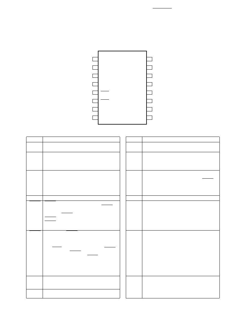
Pin Descriptions
Symbol
V
IN+
Non-inverting gate drive voltage output
(
V
OUT
) control input.
V
IN-
Inverting gate drive voltage output
(
V
OUT
) control input.
Description
Symbol
V
E
Description
Common (IGBT emitter) output supply
voltage.
LED 2 anode. This pin must be left uncon-
nected for guaranteed data sheet
performance. (For optical coupling testing
only)
Desaturation voltage input. When the voltage
on DESAT exceeds an internal reference
voltage of 7 V while the IGBT is on, FAULT
output is changed from a high impedance
state to a logic low state within 5
μ
s. See
Note 25.
Positive output supply voltage.
Collector of output pull-up triple-darlington
transistor. It is connected to V
CC2
directly or
through a resistor to limit output turn-on
current.
V
LED2+
V
CC1
Positive input supply voltage. (4.5 V to 5.5 V)
DESAT
GND1
RESET
Input Ground.
FAULT reset input. A logic low input for at
least 0.1
μ
s, asynchronously resets FAULT
output high and enables V
IN
. Synchronous
control of RESET relative to V
IN
is required.
RESET is not affected by UVLO. Asserting
RESET while V
OUT
is high does not affect
V
OUT
.
Fault output. FAULT changes from a high
impedance state to a logic low output within
5
μ
s of the voltage on the DESAT pin
exceeding an internal reference voltage of
7 V. FAULT output remains low until RESET
is brought low. FAULT output is an open
collector which allows the FAULT outputs
from all HCPL-316Js in a circuit
to be connected together in a “wired OR”
forming a single fault bus for interfacing
directly to the micro-controller.
LED 1 anode. This pin must be left uncon-
nected for guaranteed data sheet per-
formance. (For optical coupling testing only)
LED 1 cathode. This pin must be connected
to ground.
V
CC2
V
C
FAULT
V
OUT
Gate drive voltage output.
V
LED1+
V
EE
Output supply voltage.
V
LED1-
Package Pin Out
16
15
14
13
12
11
10
9
1
2
3
4
5
6
7
8
V
E
V
LED2+
DESAT
V
CC2
V
C
V
OUT
V
EE
V
EE
V
IN+
V
IN-
V
CC1
GND1
RESET
FAULT
V
LED1+
V
LED1-
相關(guān)PDF資料 |
PDF描述 |
|---|---|
| HCPL-3700 | AC/DC to Logic Interface Optocouplers(AC/DC邏輯接口光耦合器) |
| HCPL-4100300 | Optically Coupled 20 mA Current Loop Transmitter |
| HCPL-4100500 | Optically Coupled 20 mA Current Loop Transmitter |
| HCPL4100 | Optically Coupled 20 mA Current Loop Transmitter |
| HCPL-4100 | Optically Coupled 20 mA Optically Coupled 20 mA |
相關(guān)代理商/技術(shù)參數(shù) |
參數(shù)描述 |
|---|---|
| HCPL-316J#500 | 功能描述:邏輯輸出光電耦合器 2.0A IGBT Gate Drive RoHS:否 制造商:Fairchild Semiconductor 絕緣電壓:4243 Vrms 輸出類型:Push-Pull 最大傳播延遲時(shí)間:500 ns 最大正向二極管電壓: 最大反向二極管電壓: 最大正向二極管電流: 最大連續(xù)輸出電流:2.5 A 最大功率耗散:100 mW 最大工作溫度:+ 100 C 最小工作溫度:- 40 C 封裝 / 箱體:SO-16 封裝:Tube |
| HCPL-316J-000E | 功能描述:邏輯輸出光電耦合器 2.0A IGBT Gate Drive RoHS:否 制造商:Fairchild Semiconductor 絕緣電壓:4243 Vrms 輸出類型:Push-Pull 最大傳播延遲時(shí)間:500 ns 最大正向二極管電壓: 最大反向二極管電壓: 最大正向二極管電流: 最大連續(xù)輸出電流:2.5 A 最大功率耗散:100 mW 最大工作溫度:+ 100 C 最小工作溫度:- 40 C 封裝 / 箱體:SO-16 封裝:Tube |
| HCPL-316J-000E | 制造商:Avago Technologies 功能描述:GATE DRIVE OPTOCOUPLERLF - LEAD FREE VE |
| HCPL-316J-500E | 功能描述:邏輯輸出光電耦合器 2.0A IGBT Gate Drive RoHS:否 制造商:Fairchild Semiconductor 絕緣電壓:4243 Vrms 輸出類型:Push-Pull 最大傳播延遲時(shí)間:500 ns 最大正向二極管電壓: 最大反向二極管電壓: 最大正向二極管電流: 最大連續(xù)輸出電流:2.5 A 最大功率耗散:100 mW 最大工作溫度:+ 100 C 最小工作溫度:- 40 C 封裝 / 箱體:SO-16 封裝:Tube |
| HCPL-3180 | 功能描述:高速光耦合器 2.0A IGBT Gate Drive RoHS:否 制造商:Avago Technologies 電流傳遞比: 最大波特率: 最大正向二極管電壓:1.75 V 最大反向二極管電壓:5 V 最大功率耗散:40 mW 最大工作溫度:+125 C 最小工作溫度:- 40 C 封裝 / 箱體:SOIC-5 封裝:Tube |
發(fā)布緊急采購(gòu),3分鐘左右您將得到回復(fù)。