- 您現(xiàn)在的位置:買賣IC網(wǎng) > PDF目錄375765 > FDB8878 (FAIRCHILD SEMICONDUCTOR CORP) N-Channel Logic Level PowerTrench㈢ MOSFET 30V, 48A, 14mOhm PDF資料下載
參數(shù)資料
| 型號(hào): | FDB8878 |
| 廠商: | FAIRCHILD SEMICONDUCTOR CORP |
| 元件分類: | JFETs |
| 英文描述: | N-Channel Logic Level PowerTrench㈢ MOSFET 30V, 48A, 14mOhm |
| 中文描述: | 48 A, 30 V, 0.014 ohm, N-CHANNEL, Si, POWER, MOSFET, TO-263AB |
| 封裝: | ROHS COMPLIANT PACKAGE-3 |
| 文件頁(yè)數(shù): | 2/6頁(yè) |
| 文件大?。?/td> | 226K |
| 代理商: | FDB8878 |
F
FDB8878 Rev. A
www.fairchildsemi.com
2
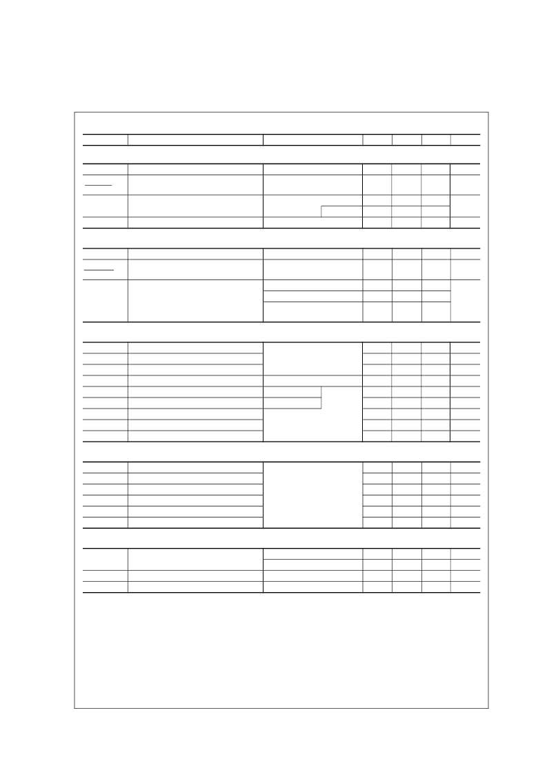
Electrical Characteristics
T
A
= 25°C unless otherwise noted
Symbol
Parameter
Test Conditions
Min
Typ
Max
Units
Off Characteristics
B
VDSS
BV
DSS
T
J
Drain to Source Breakdown Voltage
I
D
= 250
μ
A, V
GS
= 0V
I
D
= 250
μ
A,
Referenced to 25
o
C
V
DS
= 24V
V
GS
= 0V
V
GS
= ±20V
30
-
-
V
Breakdown Voltage Temp. Coefficient
21
mV/
o
C
I
DSS
Zero Gate Voltage Drain Current
-
-
-
-
-
-
1
μ
A
T
A
= 150
o
C
250
±100
I
GSS
Gate to Source Leakage Current
nA
On Characteristics
V
GS(TH)
V
GS(TH)
T
J
Gate to Source Threshold Voltage
Gate to Source Threshold Voltage
Temperature Coefficient
V
GS
= V
DS
, I
D
= 250
μ
A
I
D
= 250
μ
A,
Referenced to 25
o
C
I
D
= 40A, V
GS
= 10V
I
D
= 36A, V
GS
= 4.5V
I
D
= 40, V
GS
= 10V,
T
A
= 175
o
C
1.2
1.7
2.5
V
-5
mV/
o
C
r
DS(ON)
Drain to Source On Resistance
-
-
12
15
14
18
m
-
19
21
Dynamic Characteristics
C
ISS
C
OSS
C
RSS
R
G
Q
g(TOT)
Q
g(5)
Q
gs
Q
gs2
Q
gd
Input Capacitance
Output Capacitance
Reverse Transfer Capacitance
Gate Resistance
Total Gate Charge at 10V
Total Gate Charge at 5V
Gate to Source Gate Charge
Gate Charge Threshold to Plateau
Gate to Drain “Miller” Charge
V
DS
= 15V, V
GS
= 0V,
f = 1MHz
-
-
-
927
188
117
3.0
17.1
9.2
2.6
1.7
3.7
1235
250
175
pF
pF
pF
nC
nC
nC
nC
nC
f = 1MHz
V
GS
= 0V to 10VV
DD
= 15V
V
GS
= 0V to 5V
I
D
= 40A
I
g
= 1.0mA
-
-
-
-
-
23
12
-
-
-
Switching Characteristics
(V
GS
= 10V)
t
ON
Turn-On Time
t
d(ON)
Turn-On Delay Time
t
r
Rise Time
t
d(OFF)
Turn-Off Delay Time
t
f
Fall Time
t
OFF
Turn-Off Time
V
DD
= 15V, I
D
= 40A
V
GS
= 10V, R
GS
= 16
-
-
-
-
-
-
255
11.1
244
14.8
35.3
50
383
ns
ns
ns
ns
ns
ns
75
Drain-Source Diode Characteristics
V
SD
Source to Drain Diode Voltage
I
SD
= 40A
I
SD
= 3.2A
I
SD
= 40A, dI
SD
/dt=100A/
μ
s
I
SD
= 40A, dI
SD
/dt=100A/
μ
s
-
-
-
-
1.1
0.85
14.4
5.1
1.25
1.2
18.8
6.7
V
V
ns
nC
t
rr
Q
RR
Reverse Recovery Time
Reverse Recovered Charge
Notes:
1:
Starting T
= 25°C, V
= 30V, V
= 10V
2:
R
is the sum of the junction-to-case and case-to-ambient thermal resistance where the case thermal reference is defined as the solder mounting surface of the
drain pins. R
is guaranteed by design while R
is determined by the user’s board design.
3:
R
is measured with 1.0 in
copper on FR-4 board
4:
Pulse Test: Pulse Width < 300
μ
s, Duty Cycle < 2.0%
相關(guān)PDF資料 |
PDF描述 |
|---|---|
| FDB8880 | N-Channel PowerTrench MOSFET |
| FDP8880 | N-Channel PowerTrench MOSFET |
| FDB8896 | N-Channel PowerTrench MOSFET 30V, 93A, 5.7 m ohm |
| FDC10-48S05W | 10 watts of output power from a 2 x 1 x 0.4 inch package |
| FDC10 | 10 watts of output power from a 2 x 1 x 0.4 inch package |
相關(guān)代理商/技術(shù)參數(shù) |
參數(shù)描述 |
|---|---|
| FDB8880 | 功能描述:MOSFET NCH PWR TRNCH MOSFET 30V 54A 11.6 OHMS RoHS:否 制造商:STMicroelectronics 晶體管極性:N-Channel 汲極/源極擊穿電壓:650 V 閘/源擊穿電壓:25 V 漏極連續(xù)電流:130 A 電阻汲極/源極 RDS(導(dǎo)通):0.014 Ohms 配置:Single 最大工作溫度: 安裝風(fēng)格:Through Hole 封裝 / 箱體:Max247 封裝:Tube |
| FDB8896 | 功能描述:MOSFET 30V N-Channel PowerTrench RoHS:否 制造商:STMicroelectronics 晶體管極性:N-Channel 汲極/源極擊穿電壓:650 V 閘/源擊穿電壓:25 V 漏極連續(xù)電流:130 A 電阻汲極/源極 RDS(導(dǎo)通):0.014 Ohms 配置:Single 最大工作溫度: 安裝風(fēng)格:Through Hole 封裝 / 箱體:Max247 封裝:Tube |
| FDB8896_08 | 制造商:FAIRCHILD 制造商全稱:Fairchild Semiconductor 功能描述:N-Channel PowerTrench㈢ MOSFET |
| FDB8896_F085 | 功能描述:MOSFET 30V N-CHAN PwrTrench RoHS:否 制造商:STMicroelectronics 晶體管極性:N-Channel 汲極/源極擊穿電壓:650 V 閘/源擊穿電壓:25 V 漏極連續(xù)電流:130 A 電阻汲極/源極 RDS(導(dǎo)通):0.014 Ohms 配置:Single 最大工作溫度: 安裝風(fēng)格:Through Hole 封裝 / 箱體:Max247 封裝:Tube |
| FDB9403 | 制造商:FAIRCHILD 制造商全稱:Fairchild Semiconductor 功能描述:N-Channel Power Trench?? MOSFET 40V, 110A, 1.2m?? |
發(fā)布緊急采購(gòu),3分鐘左右您將得到回復(fù)。