- 您現(xiàn)在的位置:買賣IC網(wǎng) > PDF目錄375760 > FCBS0650 (FAIRCHILD SEMICONDUCTOR CORP) Smart Power Module (SPM) PDF資料下載
參數(shù)資料
| 型號(hào): | FCBS0650 |
| 廠商: | FAIRCHILD SEMICONDUCTOR CORP |
| 元件分類: | 運(yùn)動(dòng)控制電子 |
| 英文描述: | Smart Power Module (SPM) |
| 中文描述: | AC MOTOR CONTROLLER, 8 A, DMA27 |
| 文件頁數(shù): | 12/16頁 |
| 文件大?。?/td> | 257K |
| 代理商: | FCBS0650 |

12
www.fairchildsemi.com
FCBS0650 Rev. A
F
Note:
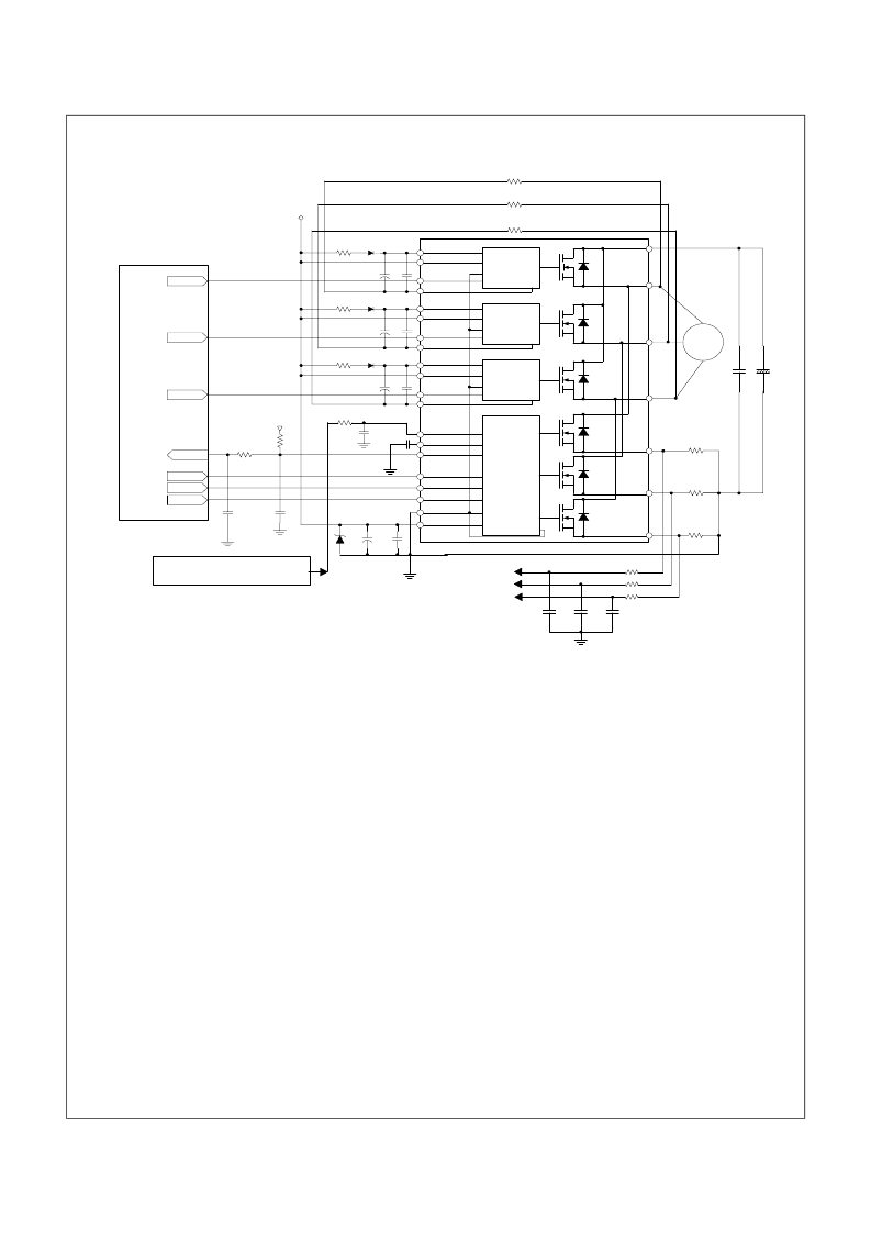
1. To avoid malfunction, the wiring of each input should be as short as possible. (less than 2-3cm)
2. By virtue of integrating an application specific type HVIC inside the SPM, direct coupling to CPU terminals without any opto-coupler or transformer isolation is possible.
3. V
FO
output is open collector type. This signal line should be pulled up to the positive side of the 5V power supply with approximately 4.7k
resistance. Please refer to Figure 9.
4. C
SP15
of around 7 times larger than bootstrap capacitor C
BS
is recommended.
5. V
output pulse width should be determined by connecting an external capacitor(C
FOD
) between C
FOD
(pin7) and COM(pin2). (Example : if C
FOD
= 33 nF, then t
FO
= 1.8ms
(typ.)) Please refer to the note 5 for calculation method.
6. Input signal is High-Active type. There is a 3.3k
resistor inside the IC to pull down each input signal line to GND. When employing RC coupling circuits, set up such RC couple
that input signal agree with turn-off/turn-on threshold voltage.
7. To prevent errors of the protection function, the wiring around R
F
and C
SC
should be as short as possible.
8. In the short-circuit protection circuit, please select the R
F
C
SC
time constant in the range 1.5~2
μ
s.
9. Each capacitor should be mounted as close to the pins of the SPM as possible.
10. To prevent surge destruction, the wiring between the smoothing capacitor and the P&COM pins should be as short as possible. The use of a high frequency non-inductive
capacitor of around 0.1~0.22
μ
F between the P&COM pins is recommended.
11. Relays are used at almost every systems of electrical equipments of home appliances. In these cases, there should be sufficient distance between the CPU and the relays.
12. C
SPC15
should be over 1
μ
F and mounted as close to the pins of the SPM as possible.
Fig. 11. Typical Application Circuit
Fault
15V line
C
BS
C
BSC
R
BS
D
BS
R
BS
D
BS
C
BS
C
BSC
R
BS
D
BS
C
FOD
5V line
R
PF
C
BPF
R
S
Vdc
C
DCS
Gating UH
Gating VH
Gating WH
Gating WL
Gating VL
Gating UL
C
PF
R
FU
R
FV
R
FW
R
SU
R
SV
R
SW
C
FU
C
FV
C
FW
W-Phase Current
V-Phase Current
U-Phase Current
R
F
COM
VCC
IN(UL)
IN(VL)
IN(WL)
VFO
C(FOD)
C(SC)
OUT(UL)
OUT(VL)
OUT(WL)
N
U
(21)
N
V
(22)
N
W
(23)
U (24)
V (25)
W (26)
P (27)
(20) V
S(W)
(19) V
B(W)
(18) V
CC(WH)
(16) V
S(V)
(15) V
B(V)
(14) V
CC(VH)
(8) C
SC
(7) C
FOD
(6) V
FO
(5) IN
(WL)
(4) IN
(VL)
(3) IN
(UL)
(2) COM
(1) V
CC(L)
VCC
COM
IN
VB
OUT
VS
VB
VCC
VS
OUT
IN
COM
VCC
COM
IN
VB
OUT
VS
(17) IN
(WH)
(13) IN
(VH)
(12) V
S(U)
(11) V
B(U)
(10) V
CC(UH)
(9) IN
(UH)
C
SC
R
E(UH)
V
SL
R
E(VH)
R
E(WH)
相關(guān)PDF資料 |
PDF描述 |
|---|---|
| FCD4B14 | Thermal Fingerprint Sensor with 0.4 mm x 14 mm Sensing Area and Digital Output |
| FCD4B14CC | Thermal Fingerprint Sensor with 0.4 mm x 14 mm Sensing Area and Digital Output |
| FCD4B14CCB | Thermal Fingerprint Sensor with 0.4 mm x 14 mm Sensing Area and Digital Output |
| FCD5N60TM | 600V N-Channel MOSFET |
| FCU5N60 | 600V N-Channel MOSFET |
相關(guān)代理商/技術(shù)參數(shù) |
參數(shù)描述 |
|---|---|
| F-CBS-F1 | 制造商:Cosel Usa Inc 功能描述:Heat Sink; Vertical; Size H 12.7mm X W 57.9mm X D 61.5mm 制造商:Cosel Usa Inc 功能描述:CBS series Heat Sink Vertical; Size H 12.7mm X W 57.9mm X D 61.5mm 制造商:Cosel Usa Inc 功能描述:Optional Accessories, OP Series |
| F-CBS-F2 | 制造商:Cosel Usa Inc 功能描述:Optional Accessories, OP Serie 制造商:Cosel Usa Inc 功能描述:Optional Accessories, OP Series |
| F-CBS-F3 | 制造商:Cosel Usa Inc 功能描述:Bulk 制造商:Cosel Usa Inc 功能描述:Optional Accessories, OP Series |
| F-CBS-F4 | 制造商:Cosel Usa Inc 功能描述:Optional Accessories, OP Series |
| F-CBS-F5 | 制造商:Cosel Usa Inc 功能描述:Optional Accessories, OP Series |
發(fā)布緊急采購,3分鐘左右您將得到回復(fù)。