- 您現(xiàn)在的位置:買賣IC網(wǎng) > PDF目錄384281 > EDS1232AABB (Elpida Memory, Inc.) 128M bits SDRAM PDF資料下載
參數(shù)資料
| 型號: | EDS1232AABB |
| 廠商: | Elpida Memory, Inc. |
| 英文描述: | 128M bits SDRAM |
| 中文描述: | 128兆位內(nèi)存 |
| 文件頁數(shù): | 7/55頁 |
| 文件大小: | 564K |
| 代理商: | EDS1232AABB |
第1頁第2頁第3頁第4頁第5頁第6頁當(dāng)前第7頁第8頁第9頁第10頁第11頁第12頁第13頁第14頁第15頁第16頁第17頁第18頁第19頁第20頁第21頁第22頁第23頁第24頁第25頁第26頁第27頁第28頁第29頁第30頁第31頁第32頁第33頁第34頁第35頁第36頁第37頁第38頁第39頁第40頁第41頁第42頁第43頁第44頁第45頁第46頁第47頁第48頁第49頁第50頁第51頁第52頁第53頁第54頁第55頁
EDS1232CABB, EDS1232CATA
Preliminary Data Sheet E0247E40 (Ver. 4.0)
7
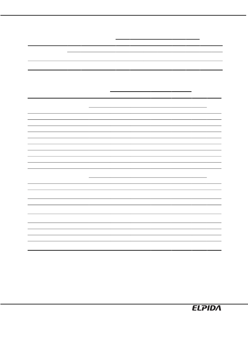
Pin Capacitance (TA = 25°C, f = 1MHz)
90-ball FBGA
86-pin TSOP (II)
Parameter
Symbol Pins
min.
Typ
max.
min.
Typ
max.
Unit
Notes
Input capacitance
CI1
Address
CLK, CKE, /CS, /RAS,
/CAS, /WE, DQM
1.5
—
3.0
2.5
—
4.0
pF
CI2
1.5
—
3.0
2.5
—
4.0
pF
Data input/output
capacitance
CI/O
DQ
3.0
—
5.5
4.0
—
6.5
pF
AC Characteristics (TA = 0 to +70
°
C, VDD, VDDQ = 2.5V
±
0.2V, VSS, VSSQ = 0V)
-75
-1A
Parameter
Symbol
min.
max.
min.
max.
Unit
Notes
System clock cycle time
(CL = 2)
(CL = 3)
tCK
10
—
10
—
ns
tCK
7.5
—
10
—
ns
CLK high pulse width
tCH
2.5
—
3
—
ns
CLK low pulse width
tCL
2.5
—
3
—
ns
Access time from CLK
tAC
—
5.4
—
6
ns
Data-out hold time
tOH
2
—
2
—
ns
CLK to Data-out low impedance
tLZ
0
—
0
—
ns
CLK to Data-out high impedance
tHZ
2
5.4
2
6
ns
Input setup time
tSI
1.5
—
2
—
ns
Input hold time
tHI
0.8
—
1
—
ns
CKE setup time (Power down exit)
ACT to REF/ACT command period
(operation)
(refresh)
tCKSP
1.5
—
2
—
ns
tRC
67.5
70
ns
tRC
67.5
70
ns
Active to Precharge command period
Active command to column command
(same bank)
Precharge to active command period
Write recovery or data-in to precharge
lead time
tRAS
45
120000
50
120000
ns
tRCD
20
20
ns
tRP
20
20
ns
tDPL
15
20
ns
Last data into active latency
tDAL
2CLK +
20ns
15
2CLK +
20ns
20
—
Active (a) to Active (b) command period tRRD
—
ns
Mode register set cycle time
tRSC
2
2
CLK
Transition time (rise and fall)
Refresh period
(4096 refresh cycles)
tT
0.5
30
0.5
30
ns
tREF
—
64
—
64
ms
相關(guān)PDF資料 |
PDF描述 |
|---|---|
| EDS1232AABB-60L-E | 128M bits SDRAM |
| EDS1232AABB-75-E | 128M bits SDRAM |
| EDS1232AASE | 26481083 |
| EDS1232AATA | 128M bits SDRAM |
| EDS1232AATA-60 | 128M bits SDRAM |
相關(guān)代理商/技術(shù)參數(shù) |
參數(shù)描述 |
|---|---|
| EDS1232AABB-60 | 制造商:未知廠家 制造商全稱:未知廠家 功能描述:SDRAM|4X1MX32|CMOS|BGA|90PIN|PLASTIC |
| EDS1232AABB-60-E | 制造商:ELPIDA 制造商全稱:Elpida Memory 功能描述:128M bits SDRAM |
| EDS1232AABB-60L | 制造商:未知廠家 制造商全稱:未知廠家 功能描述:SDRAM|4X1MX32|CMOS|BGA|90PIN|PLASTIC |
| EDS1232AABB-60L-E | 制造商:ELPIDA 制造商全稱:Elpida Memory 功能描述:128M bits SDRAM |
| EDS1232AABB-75 | 制造商:未知廠家 制造商全稱:未知廠家 功能描述:SDRAM|4X1MX32|CMOS|BGA|90PIN|PLASTIC |
發(fā)布緊急采購,3分鐘左右您將得到回復(fù)。