- 您現(xiàn)在的位置:買(mǎi)賣(mài)IC網(wǎng) > PDF目錄1917 > DSP56303VL100B1 (Freescale Semiconductor)IC DSP 24BIT 100MHZ 196-BGA PDF資料下載
參數(shù)資料
| 型號(hào): | DSP56303VL100B1 |
| 廠商: | Freescale Semiconductor |
| 文件頁(yè)數(shù): | 20/108頁(yè) |
| 文件大小: | 0K |
| 描述: | IC DSP 24BIT 100MHZ 196-BGA |
| 標(biāo)準(zhǔn)包裝: | 630 |
| 系列: | DSP563xx |
| 類(lèi)型: | 定點(diǎn) |
| 接口: | 主機(jī)接口,SSI,SCI |
| 時(shí)鐘速率: | 100MHz |
| 非易失內(nèi)存: | ROM(576 B) |
| 芯片上RAM: | 24kB |
| 電壓 - 輸入/輸出: | 3.30V |
| 電壓 - 核心: | 3.30V |
| 工作溫度: | -40°C ~ 100°C |
| 安裝類(lèi)型: | 表面貼裝 |
| 封裝/外殼: | 196-LBGA |
| 供應(yīng)商設(shè)備封裝: | 196-MAPBGA(15x15) |
| 包裝: | 托盤(pán) |
第1頁(yè)第2頁(yè)第3頁(yè)第4頁(yè)第5頁(yè)第6頁(yè)第7頁(yè)第8頁(yè)第9頁(yè)第10頁(yè)第11頁(yè)第12頁(yè)第13頁(yè)第14頁(yè)第15頁(yè)第16頁(yè)第17頁(yè)第18頁(yè)第19頁(yè)當(dāng)前第20頁(yè)第21頁(yè)第22頁(yè)第23頁(yè)第24頁(yè)第25頁(yè)第26頁(yè)第27頁(yè)第28頁(yè)第29頁(yè)第30頁(yè)第31頁(yè)第32頁(yè)第33頁(yè)第34頁(yè)第35頁(yè)第36頁(yè)第37頁(yè)第38頁(yè)第39頁(yè)第40頁(yè)第41頁(yè)第42頁(yè)第43頁(yè)第44頁(yè)第45頁(yè)第46頁(yè)第47頁(yè)第48頁(yè)第49頁(yè)第50頁(yè)第51頁(yè)第52頁(yè)第53頁(yè)第54頁(yè)第55頁(yè)第56頁(yè)第57頁(yè)第58頁(yè)第59頁(yè)第60頁(yè)第61頁(yè)第62頁(yè)第63頁(yè)第64頁(yè)第65頁(yè)第66頁(yè)第67頁(yè)第68頁(yè)第69頁(yè)第70頁(yè)第71頁(yè)第72頁(yè)第73頁(yè)第74頁(yè)第75頁(yè)第76頁(yè)第77頁(yè)第78頁(yè)第79頁(yè)第80頁(yè)第81頁(yè)第82頁(yè)第83頁(yè)第84頁(yè)第85頁(yè)第86頁(yè)第87頁(yè)第88頁(yè)第89頁(yè)第90頁(yè)第91頁(yè)第92頁(yè)第93頁(yè)第94頁(yè)第95頁(yè)第96頁(yè)第97頁(yè)第98頁(yè)第99頁(yè)第100頁(yè)第101頁(yè)第102頁(yè)第103頁(yè)第104頁(yè)第105頁(yè)第106頁(yè)第107頁(yè)第108頁(yè)
Timers
DSP56303 Technical Data, Rev. 11
Freescale Semiconductor
1-15
1.11 Timers
The DSP56303 has three identical and independent timers. Each timer can use internal or external clocking and can
either interrupt the DSP56303 after a specified number of events (clocks) or signal an external device after
counting a specific number of internal events.
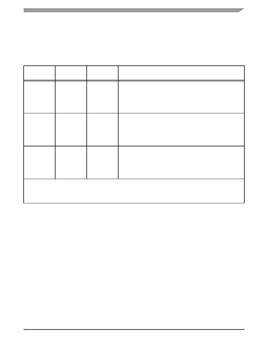
Table 1-15.
Triple Timer Signals
Signal Name
Type
State During
Reset1,2
Signal Description
TIO0
Input or Output
Ignored Input
Timer 0 Schmitt-Trigger Input/Output— When Timer 0 functions as an
external event counter or in measurement mode, TIO0 is used as input. When
Timer 0 functions in watchdog, timer, or pulse modulation mode, TIO0 is used
as output.
The default mode after reset is GPIO input. TIO0 can be changed to output or
configured as a timer I/O through the Timer 0 Control/Status Register (TCSR0).
TIO1
Input or Output
Ignored Input
Timer 1 Schmitt-Trigger Input/Output— When Timer 1 functions as an
external event counter or in measurement mode, TIO1 is used as input. When
Timer 1 functions in watchdog, timer, or pulse modulation mode, TIO1 is used
as output.
The default mode after reset is GPIO input. TIO1 can be changed to output or
configured as a timer I/O through the Timer 1 Control/Status Register (TCSR1).
TIO2
Input or Output
Ignored Input
Timer 2 Schmitt-Trigger Input/Output— When Timer 2 functions as an
external event counter or in measurement mode, TIO2 is used as input. When
Timer 2 functions in watchdog, timer, or pulse modulation mode, TIO2 is used
as output.
The default mode after reset is GPIO input. TIO2 can be changed to output or
configured as a timer I/O through the Timer 2 Control/Status Register (TCSR2).
Notes:
1.
In the Stop state, the signal maintains the last state as follows:
If the last state is input, the signal is an ignored input.
If the last state is output, the signal is tri-stated.
2.
The Wait processing state does not affect the signal state.
3.
All inputs are 5 V tolerant.
相關(guān)PDF資料 |
PDF描述 |
|---|---|
| DSP56311VF150B1 | IC DSP 24BIT 150MHZ 196-BGA |
| DSP56321VF200R2 | IC DSP 24BIT 200MHZ 196-BGA |
| DSP56852VFE | IC DSP 16BIT 120MHZ 81-MAPBGA |
| DSP56854FGE | IC DSP 16BIT 120MHZ 128-LQFP |
| DSP56855BUE | IC DSP 16BIT 120MHZ 100-LQFP |
相關(guān)代理商/技術(shù)參數(shù) |
參數(shù)描述 |
|---|---|
| DSP56304GC66 | 制造商:未知廠家 制造商全稱(chēng):未知廠家 功能描述:24-Bit Digital Signal Processor |
| DSP56304GC80 | 制造商:未知廠家 制造商全稱(chēng):未知廠家 功能描述:24-Bit Digital Signal Processor |
| DSP56304PV66 | 制造商:未知廠家 制造商全稱(chēng):未知廠家 功能描述:24-Bit Digital Signal Processor |
| DSP56304PV80 | 制造商:未知廠家 制造商全稱(chēng):未知廠家 功能描述:24-Bit Digital Signal Processor |
| DSP56305DS | 制造商:未知廠家 制造商全稱(chēng):未知廠家 功能描述:DSP56305 Single Chip Channel Codec Digital Signal Processor Data Sheet |
發(fā)布緊急采購(gòu),3分鐘左右您將得到回復(fù)。