- 您現(xiàn)在的位置:買賣IC網(wǎng) > PDF目錄97868 > DS232AS (DALLAS SEMICONDUCTOR) LINE TRANSCEIVER, PDSO16 PDF資料下載
參數(shù)資料
| 型號: | DS232AS |
| 廠商: | DALLAS SEMICONDUCTOR |
| 元件分類: | Line Driver or Receiver |
| 英文描述: | LINE TRANSCEIVER, PDSO16 |
| 封裝: | 0.300 INCH, SOIC-16 |
| 文件頁數(shù): | 8/28頁 |
| 文件大小: | 581K |
| 代理商: | DS232AS |
第1頁第2頁第3頁第4頁第5頁第6頁第7頁當(dāng)前第8頁第9頁第10頁第11頁第12頁第13頁第14頁第15頁第16頁第17頁第18頁第19頁第20頁第21頁第22頁第23頁第24頁第25頁第26頁第27頁第28頁
MAX15023
Wide 4.5V to 28V Input, Dual-Output
Synchronous Buck Controller
16
Maxim Integrated
In case of a nonideal short circuit applied at the output,
the output voltage equals the output impedance times the
limited inductor current during this phase. After reaching
the maximum allowable limit of the soft-start duration
(twice the normal soft-start time), the controller remains off
for 7936 clock cycles before trying to soft-start again.
Undervoltage Lockout
The MAX15023 has an internal undervoltage lockout
(UVLO) circuit to monitor the voltage on VCC. The
UVLO circuit prevents the MAX15023 from operating if
the voltages for the MOSFET drivers or for the internal
control functions are too low. The VCC falling threshold
is 3.8V (typ), with 430mV hysteresis to prevent chatter-
ing on the rising/falling edge of the supply voltage.
Before VCC reaches UVLO rising threshold voltage,
DL_ and DH_ stay low to inhibit switching.
Thermal-Overload Protection
Thermal-overload protection limits total power dissipation
in the MAX15023. When the device’s die-junction tem-
perature exceeds TJ = +150°C, an on-chip thermal sen-
sor shuts down the device, forcing DL_ and DH_ low,
allowing the IC to cool. The thermal sensor turns the
device on again after the junction temperature cools by
20°C. During thermal shutdown, the regulators shut
down, and soft-start is reset. Thermal-overload protection
can be triggered by power dissipation in the LDO regula-
tor, by excessive driving losses, or by both. Therefore,
carefully evaluate the total power dissipation (see the
Power Dissipation section) to avoid unwanted triggering
of the thermal-overload protection in normal operation.
Design Procedure
Effective Input Voltage Range
Although the MAX15023 controllers can operate from
input supplies up to 28V and regulate down to 0.6V, the
minimum voltage conversion ratio (VOUT/VIN) might be
limited by the minimum controllable on-time. For proper
fixed-frequency PWM operation, the voltage conversion
ratio should obey the following condition:
where tON(MIN) is 100ns (max) and fSW is the switching
frequency in Hertz. If the desired voltage conversion
does not meet the above condition, then pulse skipping
occurs to decrease the effective duty cycle. To avoid
this, decrease the switching frequency or lower the
input voltage VIN.
The maximum voltage conversion ratio is limited by the
maximum duty cycle (Dmax):
where VDROP1 is the sum of the parasitic voltage drops
in the inductor discharge path, including synchronous
rectifier, inductor, and PCB resistances. VDROP2 is the
sum of the voltage drops in the charging path, includ-
ing high-side switch, inductor, and PCB resistances. In
practice, the above condition should be met with ade-
quate margin for good load-transient response.
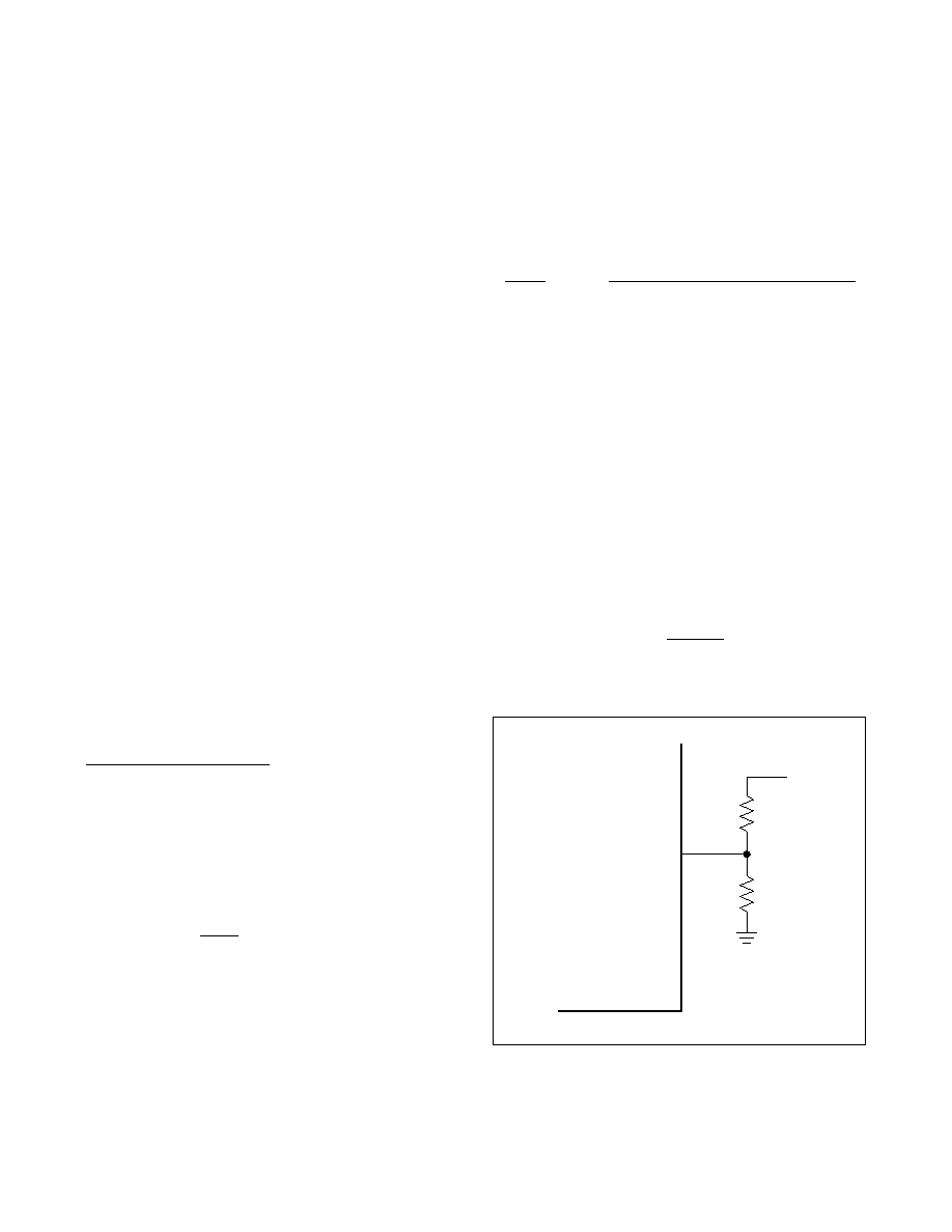
Setting the Enable Input (EN_)
Each controller has an enable input referenced to an
analog voltage (1.2V). When the voltage exceeds 1.2V,
the regulator is enabled. To set a specific turn-on
threshold that can act as a secondary UVLO, a resistive
divider circuit can be used (see Figure 2)
Select R2 (EN_ to SGND resistor) to a value lower than
200k
. Calculate R1 (VMON to EN_ resistor) with the fol-
lowing equation:
where VEN_H_ = 1.2V (typical).
RR
V
MON
EN H
12
1
=
__
V
D
V
(1 D
)
V
OUT
IN
max
DROP2
max
DROP1
IN
<
×+
×
V
tf
OUT
N
ON(MIN)
SW
I
>×
EN_
R1
VMON
R2
MA15023
Figure 2. Adjustable Enable Voltage
相關(guān)PDF資料 |
PDF描述 |
|---|---|
| DS232A | LINE TRANSCEIVER, PDIP16 |
| DS2404S-001 | 0 TIMER(S), REAL TIME CLOCK, PDSO16 |
| DS2404B | 0 TIMER(S), REAL TIME CLOCK, PDSO16 |
| DS2404 | 0 TIMER(S), REAL TIME CLOCK, PDIP16 |
| DS2405P | SPECIALTY MEMORY CIRCUIT, PDSO6 |
相關(guān)代理商/技術(shù)參數(shù) |
參數(shù)描述 |
|---|---|
| DS232AS/T&R | 制造商:Maxim Integrated Products 功能描述:IC TXRX DUAL RS-232 5V 16-SOIC |
| DS232AS/T&R | 功能描述:RS-232接口集成電路 RoHS:否 制造商:Exar 數(shù)據(jù)速率:52 Mbps 工作電源電壓:5 V 電源電流:300 mA 工作溫度范圍:- 40 C to + 85 C 安裝風(fēng)格:SMD/SMT 封裝 / 箱體:LQFP-100 封裝: |
| DS232AS+ | 功能描述:RS-232接口集成電路 Dual RS-232 Transmitter/Receiver RoHS:否 制造商:Exar 數(shù)據(jù)速率:52 Mbps 工作電源電壓:5 V 電源電流:300 mA 工作溫度范圍:- 40 C to + 85 C 安裝風(fēng)格:SMD/SMT 封裝 / 箱體:LQFP-100 封裝: |
| DS232AS+T&R | 制造商:Maxim Integrated Products 功能描述:IC TXRX DUAL RS-232 5V 16-SOIC |
| DS232AS+T&R | 功能描述:RS-232接口集成電路 RoHS:否 制造商:Exar 數(shù)據(jù)速率:52 Mbps 工作電源電壓:5 V 電源電流:300 mA 工作溫度范圍:- 40 C to + 85 C 安裝風(fēng)格:SMD/SMT 封裝 / 箱體:LQFP-100 封裝: |
發(fā)布緊急采購,3分鐘左右您將得到回復(fù)。