- 您現(xiàn)在的位置:買賣IC網(wǎng) > PDF目錄97865 > DS18S20Z/T&R (MAXIM INTEGRATED PRODUCTS INC) DIGITAL TEMP SENSOR-SERIAL, 9BIT(s), 0.50Cel, RECTANGULAR, SURFACE MOUNT PDF資料下載
參數(shù)資料
| 型號: | DS18S20Z/T&R |
| 廠商: | MAXIM INTEGRATED PRODUCTS INC |
| 元件分類: | Switch/Digital Output Temperature Sensor |
| 英文描述: | DIGITAL TEMP SENSOR-SERIAL, 9BIT(s), 0.50Cel, RECTANGULAR, SURFACE MOUNT |
| 封裝: | SOP-8 |
| 文件頁數(shù): | 13/23頁 |
| 文件大小: | 252K |
| 代理商: | DS18S20Z/T&R |
DS18S20
20 of 23
ABSOLUTE MAXIMUM RATINGS
Voltage Range on Any Pin Relative to Ground........................................................................................-0.5V to +6.0V
Continuous Power Dissipation (TA = +70°C)
8-Pin SO (derate 5.9mW/
°C above +70°C)..........................................................................................470.6mW
3-Pin TO-92 (derate 6.3mW/
°C above +70°C).....................................................................................500mW
Operating Temperature Range ................................................................................................................-55
°C to +125°C
Storage Temperature Range....................................................................................................................-55
°C to +125°C
Lead Temperature (soldering, 10s)..........................................................................................................+260
°C
Soldering Temperature (reflow)
Lead(Pb)-free ......................................................................................................................................+260
°C
Containing lead(Pb) ............................................................................................................................+240
°C
These are stress ratings only and functional operation of the device at these or any other conditions above those indicated in the operation sections of this
specification is not implied. Exposure to absolute maximum rating conditions for extended periods of time may affect reliability.
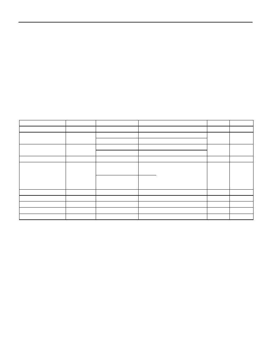
DC ELECTRICAL CHARACTERISTICS
(VDD = 3.0V to 5.5V, TA = -55°C to +125°C, unless otherwise noted.)
PARAMETER
SYMBOL
CONDITIONS
MIN
TYP
MAX
UNITS
NOTES
Supply Voltage
VDD
Local Power
+3.0
+5.5
V
1
Pullup Supply
Voltage
VPU
Parasite Power
+3.0
+5.5
V
1, 2
Local Power
+3.0
VDD
Thermometer Error
tERR
-10°C to +85°C
±0.5
°C
3
-55°C to +125°C
±2
Input Logic-Low
VIL
-0.3
+0.8
V
1, 4, 5
Input Logic-High
VIH
Local Power
+2.2
The lower of
5.5
or
VDD + 0.3
V
1, 6
Parasite Power
+3.0
Sink Current
IL
VI/O = 0.4V
4.0
mA
1
Standby Current
IDDS
750
1000
nA
7, 8
Active Current
IDD
VDD = 5V
1
1.5
mA
9
DQ Input Current
IDQ
5
A
10
Drift
±0.2
°C
11
NOTES:
1) All voltages are referenced to ground.
2) The Pullup Supply Voltage specification assumes that the pullup device is ideal, and therefore the high level of
the pullup is equal to VPU. In order to meet the VIH spec of the DS18S20, the actual supply rail for the strong
pullup transistor must include margin for the voltage drop across the transistor when it is turned on; thus:
VPU_ACTUAL = VPU_IDEAL + VTRANSISTOR.
3) See typical performance curve in
4) Logic-low voltages are specified at a sink current of 4mA.
5) To guarantee a presence pulse under low voltage parasite power conditions, VILMAX may have to be reduced to
as low as 0.5V.
6) Logic-high voltages are specified at a source current of 1mA.
7) Standby current specified up to +70
°C. Standby current typically is 3A at +125°C.
8) To minimize IDDS, DQ should be within the following ranges: GND ≤ DQ ≤ GND + 0.3V or
VDD – 0.3V ≤ DQ ≤ VDD.
9) Active current refers to supply current during active temperature conversions or EEPROM writes.
10) DQ line is high (“high-Z” state).
11) Drift data is based on a 1000-hour stress test at +125°C with VDD = 5.5V.
相關(guān)PDF資料 |
PDF描述 |
|---|---|
| DS1963L-F5 | SPECIALTY MEMORY CIRCUIT, MEDB2 |
| DS1963S | SPECIALTY MEMORY CIRCUIT, MEDB2 |
| DS1985-F3 | 2K X 8 EEPROM 3V, RDB2 |
| DS1986-F3 | 64K X 1 OTPROM, MEDB2 |
| DS1986-F5 | 64K X 1 OTPROM, MADB2 |
相關(guān)代理商/技術(shù)參數(shù) |
參數(shù)描述 |
|---|---|
| DS18VN6LPQ | 制造商:Banner Engineering 功能描述:SENSOR, PHOTOELECTRIC, DS18VN6LPQ PICO QP NPN POL RET |
| DS18VP6FF50Q8 | 制造商:Banner Engineering 功能描述:DS18VP6FF50Q8 EURO QD PNP 50MM FIXED FIELD |
| DS18VP6LP-29537 | 制造商:Banner Engineering 功能描述:DS18 Series: Polarized Retro, Range: 3.5 m, Input: 10-30V dc, Output: Complement |
| DS18VP6LPQ8 | 制造商:Banner Engineering 功能描述:SENSOR, PHOTOELECTRIC, DS18VP6LPQ8 EURO QD PNP POL RETRO |
| DS1904 | 制造商:MAXIM 制造商全稱:Maxim Integrated Products 功能描述:Real-Time Clock/calendar in binary format RTC iButton Over 10 years of operation |
發(fā)布緊急采購,3分鐘左右您將得到回復(fù)。