- 您現(xiàn)在的位置:買賣IC網(wǎng) > PDF目錄376722 > DJIXELAD0SE001 (Intel Corp.) Advanced 8-Port 10/100 Mbps PHY Transceivers PDF資料下載
參數(shù)資料
| 型號(hào): | DJIXELAD0SE001 |
| 廠商: | Intel Corp. |
| 英文描述: | Advanced 8-Port 10/100 Mbps PHY Transceivers |
| 中文描述: | 先進(jìn)的8端口10/100 Mbps的物理層收發(fā)器 |
| 文件頁(yè)數(shù): | 45/226頁(yè) |
| 文件大小: | 1575K |
| 代理商: | DJIXELAD0SE001 |
第1頁(yè)第2頁(yè)第3頁(yè)第4頁(yè)第5頁(yè)第6頁(yè)第7頁(yè)第8頁(yè)第9頁(yè)第10頁(yè)第11頁(yè)第12頁(yè)第13頁(yè)第14頁(yè)第15頁(yè)第16頁(yè)第17頁(yè)第18頁(yè)第19頁(yè)第20頁(yè)第21頁(yè)第22頁(yè)第23頁(yè)第24頁(yè)第25頁(yè)第26頁(yè)第27頁(yè)第28頁(yè)第29頁(yè)第30頁(yè)第31頁(yè)第32頁(yè)第33頁(yè)第34頁(yè)第35頁(yè)第36頁(yè)第37頁(yè)第38頁(yè)第39頁(yè)第40頁(yè)第41頁(yè)第42頁(yè)第43頁(yè)第44頁(yè)當(dāng)前第45頁(yè)第46頁(yè)第47頁(yè)第48頁(yè)第49頁(yè)第50頁(yè)第51頁(yè)第52頁(yè)第53頁(yè)第54頁(yè)第55頁(yè)第56頁(yè)第57頁(yè)第58頁(yè)第59頁(yè)第60頁(yè)第61頁(yè)第62頁(yè)第63頁(yè)第64頁(yè)第65頁(yè)第66頁(yè)第67頁(yè)第68頁(yè)第69頁(yè)第70頁(yè)第71頁(yè)第72頁(yè)第73頁(yè)第74頁(yè)第75頁(yè)第76頁(yè)第77頁(yè)第78頁(yè)第79頁(yè)第80頁(yè)第81頁(yè)第82頁(yè)第83頁(yè)第84頁(yè)第85頁(yè)第86頁(yè)第87頁(yè)第88頁(yè)第89頁(yè)第90頁(yè)第91頁(yè)第92頁(yè)第93頁(yè)第94頁(yè)第95頁(yè)第96頁(yè)第97頁(yè)第98頁(yè)第99頁(yè)第100頁(yè)第101頁(yè)第102頁(yè)第103頁(yè)第104頁(yè)第105頁(yè)第106頁(yè)第107頁(yè)第108頁(yè)第109頁(yè)第110頁(yè)第111頁(yè)第112頁(yè)第113頁(yè)第114頁(yè)第115頁(yè)第116頁(yè)第117頁(yè)第118頁(yè)第119頁(yè)第120頁(yè)第121頁(yè)第122頁(yè)第123頁(yè)第124頁(yè)第125頁(yè)第126頁(yè)第127頁(yè)第128頁(yè)第129頁(yè)第130頁(yè)第131頁(yè)第132頁(yè)第133頁(yè)第134頁(yè)第135頁(yè)第136頁(yè)第137頁(yè)第138頁(yè)第139頁(yè)第140頁(yè)第141頁(yè)第142頁(yè)第143頁(yè)第144頁(yè)第145頁(yè)第146頁(yè)第147頁(yè)第148頁(yè)第149頁(yè)第150頁(yè)第151頁(yè)第152頁(yè)第153頁(yè)第154頁(yè)第155頁(yè)第156頁(yè)第157頁(yè)第158頁(yè)第159頁(yè)第160頁(yè)第161頁(yè)第162頁(yè)第163頁(yè)第164頁(yè)第165頁(yè)第166頁(yè)第167頁(yè)第168頁(yè)第169頁(yè)第170頁(yè)第171頁(yè)第172頁(yè)第173頁(yè)第174頁(yè)第175頁(yè)第176頁(yè)第177頁(yè)第178頁(yè)第179頁(yè)第180頁(yè)第181頁(yè)第182頁(yè)第183頁(yè)第184頁(yè)第185頁(yè)第186頁(yè)第187頁(yè)第188頁(yè)第189頁(yè)第190頁(yè)第191頁(yè)第192頁(yè)第193頁(yè)第194頁(yè)第195頁(yè)第196頁(yè)第197頁(yè)第198頁(yè)第199頁(yè)第200頁(yè)第201頁(yè)第202頁(yè)第203頁(yè)第204頁(yè)第205頁(yè)第206頁(yè)第207頁(yè)第208頁(yè)第209頁(yè)第210頁(yè)第211頁(yè)第212頁(yè)第213頁(yè)第214頁(yè)第215頁(yè)第216頁(yè)第217頁(yè)第218頁(yè)第219頁(yè)第220頁(yè)第221頁(yè)第222頁(yè)第223頁(yè)第224頁(yè)第225頁(yè)第226頁(yè)
LXT9785 and LXT9785E Advanced 8-Port 10/100 Mbps PHY Transceivers
Datasheet
Document Number: 249241
Revision Number: 007
Revision Date: August 28, 2003
47
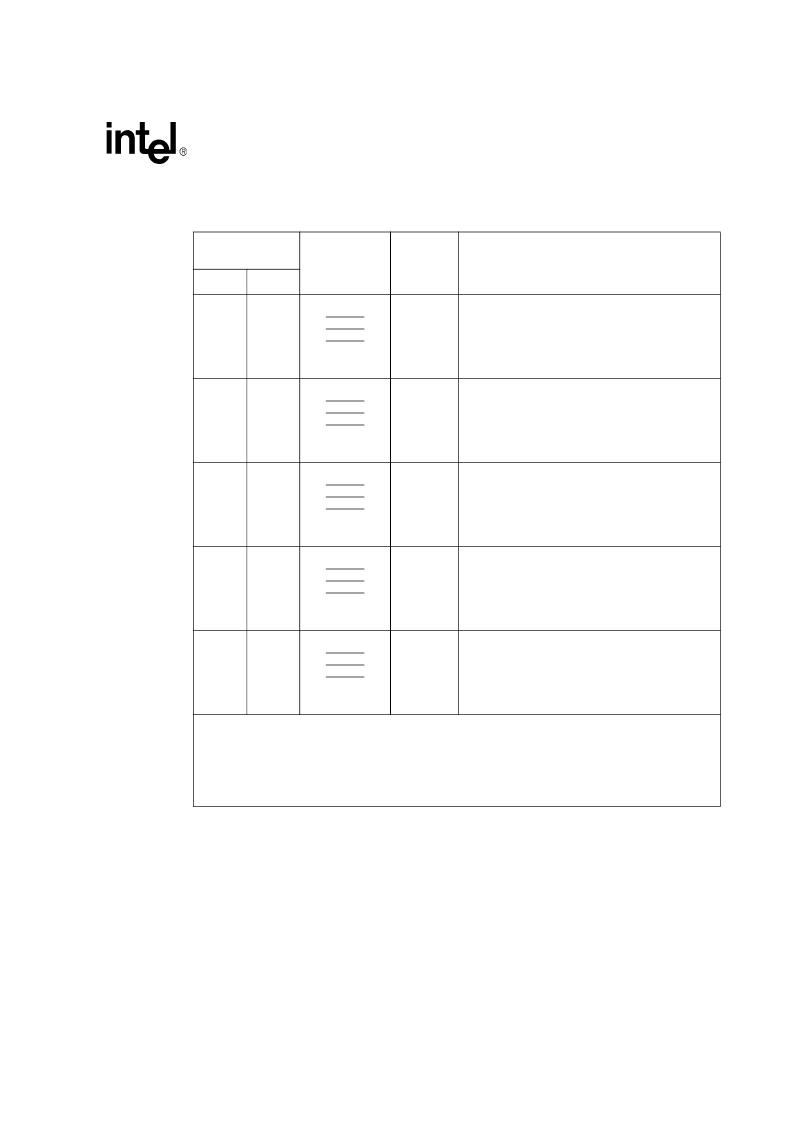
Table 14. Intel
LXT9785/LXT9785E LED Signal Descriptions – PQFP (Sheet 1 of 2)
Pin/Ball
Designation
Symbol
Type
1
Signal Description
2,3
PQFP
PBGA
82
81
80
K3,
K2,
J1
LED0_1
LED0_2
LED0_3
OD, TS, SL,
IP
Port 0 LED Drivers 1-3.
These pins drive LED indicators for Port 0. Each LED
can display one of several available status conditions
as selected by the LED Configuration Register (refer
to
Table 96, “LED Configuration Register (Address
20, Hex 14)” on page 213
for details).
77
76
75
J4,
J3,
H1
LED1_1
LED1_2
LED1_3
OD, TS, SL,
IP
Port 1 LED Drivers 1-3.
These pins drive LED indicators for Port 1. Each LED
can display one of several available status conditions
as selected by the LED Configuration Register (refer
to
Table 96, “LED Configuration Register (Address
20, Hex 14)” on page 213
for details).
73
72
71
H2,
H3,
G1
LED2_1
LED2_2
LED2_3
OD, TS, SL,
IP
Port 2 LED Drivers 1-3.
These pins drive LED indicators for Port 2. Each LED
can display one of several available status conditions
as selected by the LED Configuration Register (refer
to
Table 96, “LED Configuration Register (Address
20, Hex 14)” on page 213
for details).
70
69
68
F2,
G3,
G4
LED3_1
LED3_2
LED3_3
OD, TS, SL,
IP
Port 3 LED Drivers 1-3.
These pins drive LED indicators for Port 3. Each LED
can display one of several available status conditions
as selected by the LED Configuration Register (refer
to
Table 96, “LED Configuration Register (Address
20, Hex 14)” on page 213
for details).
180
181
182
K16,
K17,
J17
LED4_1
LED4_2
LED4_3
OD, TS, SL,
IP
Port 4 LED Drivers 1-3.
These pins drive LED indicators for Port 4. Each LED
can display one of several available status conditions
as selected by the LED Configuration Register (refer
to
Table 96, “LED Configuration Register (Address
20, Hex 14)” on page 213
for details).
1. Type Column Coding: I = Input, O = Output, OD = Open Drain output, ST = Schmitt Triggered input, TS =
Three-State-able output, SL = Slew-rate Limited output, IP = weak Internal Pull-up, ID = weak Internal pull-
Down.
2. The IP/ID resistors are disabled during H/W Power-Down mode. If a pin is an output or an I/O, the IP/ID
resistors are also disabled when the output is enabled.
3. The LED outputs are three-stated in H/W Power-Down mode and during H/W reset.
4.
相關(guān)PDF資料 |
PDF描述 |
|---|---|
| DJIXELCD0QE001 | Advanced 8-Port 10/100 Mbps PHY Transceivers |
| DJIXELCD0SE000 | Advanced 8-Port 10/100 Mbps PHY Transceivers |
| DJIXELCD0SE001 | Advanced 8-Port 10/100 Mbps PHY Transceivers |
| DJIXELED0QE000 | Advanced 8-Port 10/100 Mbps PHY Transceivers |
| DJIXELED0QE001 | Advanced 8-Port 10/100 Mbps PHY Transceivers |
相關(guān)代理商/技術(shù)參數(shù) |
參數(shù)描述 |
|---|---|
| DJIXELCD0QE000 | 制造商:INTEL 制造商全稱:Intel Corporation 功能描述:Advanced 8-Port 10/100 Mbps PHY Transceivers |
| DJIXELCD0QE001 | 制造商:INTEL 制造商全稱:Intel Corporation 功能描述:Advanced 8-Port 10/100 Mbps PHY Transceivers |
| DJIXELCD0SE000 | 制造商:INTEL 制造商全稱:Intel Corporation 功能描述:Advanced 8-Port 10/100 Mbps PHY Transceivers |
| DJIXELCD0SE001 | 制造商:INTEL 制造商全稱:Intel Corporation 功能描述:Advanced 8-Port 10/100 Mbps PHY Transceivers |
| DJIXELED0QE000 | 制造商:INTEL 制造商全稱:Intel Corporation 功能描述:Advanced 8-Port 10/100 Mbps PHY Transceivers |
發(fā)布緊急采購(gòu),3分鐘左右您將得到回復(fù)。