- 您現(xiàn)在的位置:買賣IC網(wǎng) > PDF目錄376722 > DJIXELAD0SE001 (Intel Corp.) Advanced 8-Port 10/100 Mbps PHY Transceivers PDF資料下載
參數(shù)資料
| 型號(hào): | DJIXELAD0SE001 |
| 廠商: | Intel Corp. |
| 英文描述: | Advanced 8-Port 10/100 Mbps PHY Transceivers |
| 中文描述: | 先進(jìn)的8端口10/100 Mbps的物理層收發(fā)器 |
| 文件頁(yè)數(shù): | 34/226頁(yè) |
| 文件大小: | 1575K |
| 代理商: | DJIXELAD0SE001 |
第1頁(yè)第2頁(yè)第3頁(yè)第4頁(yè)第5頁(yè)第6頁(yè)第7頁(yè)第8頁(yè)第9頁(yè)第10頁(yè)第11頁(yè)第12頁(yè)第13頁(yè)第14頁(yè)第15頁(yè)第16頁(yè)第17頁(yè)第18頁(yè)第19頁(yè)第20頁(yè)第21頁(yè)第22頁(yè)第23頁(yè)第24頁(yè)第25頁(yè)第26頁(yè)第27頁(yè)第28頁(yè)第29頁(yè)第30頁(yè)第31頁(yè)第32頁(yè)第33頁(yè)當(dāng)前第34頁(yè)第35頁(yè)第36頁(yè)第37頁(yè)第38頁(yè)第39頁(yè)第40頁(yè)第41頁(yè)第42頁(yè)第43頁(yè)第44頁(yè)第45頁(yè)第46頁(yè)第47頁(yè)第48頁(yè)第49頁(yè)第50頁(yè)第51頁(yè)第52頁(yè)第53頁(yè)第54頁(yè)第55頁(yè)第56頁(yè)第57頁(yè)第58頁(yè)第59頁(yè)第60頁(yè)第61頁(yè)第62頁(yè)第63頁(yè)第64頁(yè)第65頁(yè)第66頁(yè)第67頁(yè)第68頁(yè)第69頁(yè)第70頁(yè)第71頁(yè)第72頁(yè)第73頁(yè)第74頁(yè)第75頁(yè)第76頁(yè)第77頁(yè)第78頁(yè)第79頁(yè)第80頁(yè)第81頁(yè)第82頁(yè)第83頁(yè)第84頁(yè)第85頁(yè)第86頁(yè)第87頁(yè)第88頁(yè)第89頁(yè)第90頁(yè)第91頁(yè)第92頁(yè)第93頁(yè)第94頁(yè)第95頁(yè)第96頁(yè)第97頁(yè)第98頁(yè)第99頁(yè)第100頁(yè)第101頁(yè)第102頁(yè)第103頁(yè)第104頁(yè)第105頁(yè)第106頁(yè)第107頁(yè)第108頁(yè)第109頁(yè)第110頁(yè)第111頁(yè)第112頁(yè)第113頁(yè)第114頁(yè)第115頁(yè)第116頁(yè)第117頁(yè)第118頁(yè)第119頁(yè)第120頁(yè)第121頁(yè)第122頁(yè)第123頁(yè)第124頁(yè)第125頁(yè)第126頁(yè)第127頁(yè)第128頁(yè)第129頁(yè)第130頁(yè)第131頁(yè)第132頁(yè)第133頁(yè)第134頁(yè)第135頁(yè)第136頁(yè)第137頁(yè)第138頁(yè)第139頁(yè)第140頁(yè)第141頁(yè)第142頁(yè)第143頁(yè)第144頁(yè)第145頁(yè)第146頁(yè)第147頁(yè)第148頁(yè)第149頁(yè)第150頁(yè)第151頁(yè)第152頁(yè)第153頁(yè)第154頁(yè)第155頁(yè)第156頁(yè)第157頁(yè)第158頁(yè)第159頁(yè)第160頁(yè)第161頁(yè)第162頁(yè)第163頁(yè)第164頁(yè)第165頁(yè)第166頁(yè)第167頁(yè)第168頁(yè)第169頁(yè)第170頁(yè)第171頁(yè)第172頁(yè)第173頁(yè)第174頁(yè)第175頁(yè)第176頁(yè)第177頁(yè)第178頁(yè)第179頁(yè)第180頁(yè)第181頁(yè)第182頁(yè)第183頁(yè)第184頁(yè)第185頁(yè)第186頁(yè)第187頁(yè)第188頁(yè)第189頁(yè)第190頁(yè)第191頁(yè)第192頁(yè)第193頁(yè)第194頁(yè)第195頁(yè)第196頁(yè)第197頁(yè)第198頁(yè)第199頁(yè)第200頁(yè)第201頁(yè)第202頁(yè)第203頁(yè)第204頁(yè)第205頁(yè)第206頁(yè)第207頁(yè)第208頁(yè)第209頁(yè)第210頁(yè)第211頁(yè)第212頁(yè)第213頁(yè)第214頁(yè)第215頁(yè)第216頁(yè)第217頁(yè)第218頁(yè)第219頁(yè)第220頁(yè)第221頁(yè)第222頁(yè)第223頁(yè)第224頁(yè)第225頁(yè)第226頁(yè)
LXT9785 and LXT9785E Advanced 8-Port 10/100 Mbps PHY Transceivers
36
Datasheet
Document Number: 249241
Revision Number: 007
Revision Date: August 28, 2003
3.2
PQFP Signal Descriptions
3.2.1
Signal Name Conventions
Signal names may contain either a port designation or a serial designation, or a combination of the
two designations. Signal naming conventions are as follows:
Port Number Only.
Individual signals that apply to a particular port are designated by the
Signal Mnemonic, immediately followed by the Port Designation. For example, Transmit
Enable signals would be identified as TxEN0, TxEN1, and TxEN2.
Serial Number Only.
A set of signals which are not tied to any specific port are designated by
the Signal Mnemonic, followed by an underscore and a serial designation. For example, a set
of three Global Configuration signals would be identified as CFG_1, CFG_2, and CFG_3.
Port and Serial Number.
In cases where each port is assigned a set of multiple signals, each
signal is designated in the following order: Signal Mnemonic, Port Designation, an
underscore, and the serial designation. For example, a set of three Port Configuration signals
would be identified as RxData0_0 and RxData0_1, RxData1_0 and RxData1_1, and
RxData2_0 and RxData2_1.
3.2.2
PQFP Signal Descriptions – RMII, SMII, and SS-SMII Configurations
Table 5
through
Table 17, “Intel LXT9785/LXT9785E Receive FIFO Depth Considerations” on
page 50
provide PQFP signal descriptions. Ball designations are included for cross-reference.
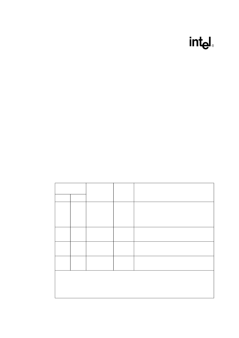
Table 5. Intel
LXT9785/LXT9785E RMII Signal Descriptions – PQFP (Sheet 1 of 3)
Pin-Ball
Designation
Symbol
Type
1
Signal Description
2,3
PQFP
PBGA
44
6
E6,
E12
REFCLK0
REFCLK1
I
Reference Clock.
50 MHz RMII reference clock is always required. RMII
inputs are sampled on the rising edge of REFCLK,
RMII outputs are sourced on the falling edge.
See
“Clock/SYNC Requirements” on page 125
for detailed
CLK requirements.
61
62
E2,
F4
TxData0_0
TxData0_1
I, ID
Transmit Data - Port 0.
Inputs containing 2-bit parallel di-bits to be transmitted
from port 0 are clocked in synchronously to REFCLK.
52
53
C3,
D4
TxData1_0
TxData1_1
I, ID
Transmit Data - Port 1.
Inputs containing 2-bit parallel di-bits to be transmitted
from port 1 are clocked in synchronously to REFCLK
42
43
B5
A4
TxData2_0
TxData2_1
I, ID
Transmit Data - Port 2.
Inputs containing 2-bit parallel di-bits to be transmitted
from port 2 are clocked in synchronously to REFCLK.
1. Type Column Coding: I = Input, O = Output, OD = Open Drain output, ST = Schmitt Triggered input, TS =
Three-State-able output, SL = Slew-rate Limited output, IP = weak Internal Pull-up, ID = weak Internal pull-
Down.
2. The IP/ID resistors are disabled during H/W Power-Down mode. If a Pin is an output or an I/O, the IP/ID
resistors are also disabled when the output is enabled.
3. RxData[0:7]_0, RxData[0:7]_1, CRS_DV[0:7] and RxER[0:7] outputs are three-stated in Isolation and H/W
Power-Down modes and during H/W reset.
相關(guān)PDF資料 |
PDF描述 |
|---|---|
| DJIXELCD0QE001 | Advanced 8-Port 10/100 Mbps PHY Transceivers |
| DJIXELCD0SE000 | Advanced 8-Port 10/100 Mbps PHY Transceivers |
| DJIXELCD0SE001 | Advanced 8-Port 10/100 Mbps PHY Transceivers |
| DJIXELED0QE000 | Advanced 8-Port 10/100 Mbps PHY Transceivers |
| DJIXELED0QE001 | Advanced 8-Port 10/100 Mbps PHY Transceivers |
相關(guān)代理商/技術(shù)參數(shù) |
參數(shù)描述 |
|---|---|
| DJIXELCD0QE000 | 制造商:INTEL 制造商全稱:Intel Corporation 功能描述:Advanced 8-Port 10/100 Mbps PHY Transceivers |
| DJIXELCD0QE001 | 制造商:INTEL 制造商全稱:Intel Corporation 功能描述:Advanced 8-Port 10/100 Mbps PHY Transceivers |
| DJIXELCD0SE000 | 制造商:INTEL 制造商全稱:Intel Corporation 功能描述:Advanced 8-Port 10/100 Mbps PHY Transceivers |
| DJIXELCD0SE001 | 制造商:INTEL 制造商全稱:Intel Corporation 功能描述:Advanced 8-Port 10/100 Mbps PHY Transceivers |
| DJIXELED0QE000 | 制造商:INTEL 制造商全稱:Intel Corporation 功能描述:Advanced 8-Port 10/100 Mbps PHY Transceivers |
發(fā)布緊急采購(gòu),3分鐘左右您將得到回復(fù)。