- 您現(xiàn)在的位置:買賣IC網(wǎng) > PDF目錄376722 > DJIXELAD0SE001 (Intel Corp.) Advanced 8-Port 10/100 Mbps PHY Transceivers PDF資料下載
參數(shù)資料
| 型號: | DJIXELAD0SE001 |
| 廠商: | Intel Corp. |
| 英文描述: | Advanced 8-Port 10/100 Mbps PHY Transceivers |
| 中文描述: | 先進的8端口10/100 Mbps的物理層收發(fā)器 |
| 文件頁數(shù): | 165/226頁 |
| 文件大小: | 1575K |
| 代理商: | DJIXELAD0SE001 |
第1頁第2頁第3頁第4頁第5頁第6頁第7頁第8頁第9頁第10頁第11頁第12頁第13頁第14頁第15頁第16頁第17頁第18頁第19頁第20頁第21頁第22頁第23頁第24頁第25頁第26頁第27頁第28頁第29頁第30頁第31頁第32頁第33頁第34頁第35頁第36頁第37頁第38頁第39頁第40頁第41頁第42頁第43頁第44頁第45頁第46頁第47頁第48頁第49頁第50頁第51頁第52頁第53頁第54頁第55頁第56頁第57頁第58頁第59頁第60頁第61頁第62頁第63頁第64頁第65頁第66頁第67頁第68頁第69頁第70頁第71頁第72頁第73頁第74頁第75頁第76頁第77頁第78頁第79頁第80頁第81頁第82頁第83頁第84頁第85頁第86頁第87頁第88頁第89頁第90頁第91頁第92頁第93頁第94頁第95頁第96頁第97頁第98頁第99頁第100頁第101頁第102頁第103頁第104頁第105頁第106頁第107頁第108頁第109頁第110頁第111頁第112頁第113頁第114頁第115頁第116頁第117頁第118頁第119頁第120頁第121頁第122頁第123頁第124頁第125頁第126頁第127頁第128頁第129頁第130頁第131頁第132頁第133頁第134頁第135頁第136頁第137頁第138頁第139頁第140頁第141頁第142頁第143頁第144頁第145頁第146頁第147頁第148頁第149頁第150頁第151頁第152頁第153頁第154頁第155頁第156頁第157頁第158頁第159頁第160頁第161頁第162頁第163頁第164頁當(dāng)前第165頁第166頁第167頁第168頁第169頁第170頁第171頁第172頁第173頁第174頁第175頁第176頁第177頁第178頁第179頁第180頁第181頁第182頁第183頁第184頁第185頁第186頁第187頁第188頁第189頁第190頁第191頁第192頁第193頁第194頁第195頁第196頁第197頁第198頁第199頁第200頁第201頁第202頁第203頁第204頁第205頁第206頁第207頁第208頁第209頁第210頁第211頁第212頁第213頁第214頁第215頁第216頁第217頁第218頁第219頁第220頁第221頁第222頁第223頁第224頁第225頁第226頁
LXT9785 and LXT9785E Advanced 8-Port 10/100 Mbps PHY Transceivers
Datasheet
Document Number: 249241
Revision Number: 007
Revision Date: August 28, 2003
167
The transmit pair should contain a balance offset in the pull-up resistors to prevent PHY-to-
fiber transceiver crosstalk amplification in power-down, loopback, and reset states (see fiber
interface application note)
The receive pair should be DC-coupled with an emitter current path for the fiber transceiver
The signal detect pin should be DC-coupled with an emitter current path for the fiber
transceiver
Refer to the fiber transceiver manufacturer’s recommendations for termination circuitry.
Figure 36
shows a typical example of an LXT9785/LXT9785E-to-3.3 V fiber transceiver interface.
The following occurs in 5 V fiber transceiver applications as shown in
Figure 37
:
The transmit pair should be AC-coupled and re-biased to 5 V PECL input levels
The transmit pair should contain a balance offset in the pull-up resistors to prevent PHY-to-
fiber transceiver crosstalk amplification in power-down, loopback, and reset states (see fiber
interface application note)
The receive pair should be AC-coupled with an emitter current path for the fiber transceiver
and re-biased to 1.2 V
The signal detect pin on a 5 V fiber transceiver interface should use the logic translator
circuitry as shown in
Figure 38
.
Refer to the fiber transceiver manufacturer’s recommendations for termination circuitry.
Figure 37
shows a typical example of an LXT9785/LXT9785E-to-5 V fiber transceiver interface, while
Figure 38
shows the interface circuitry for the logic translator.
5.2.6
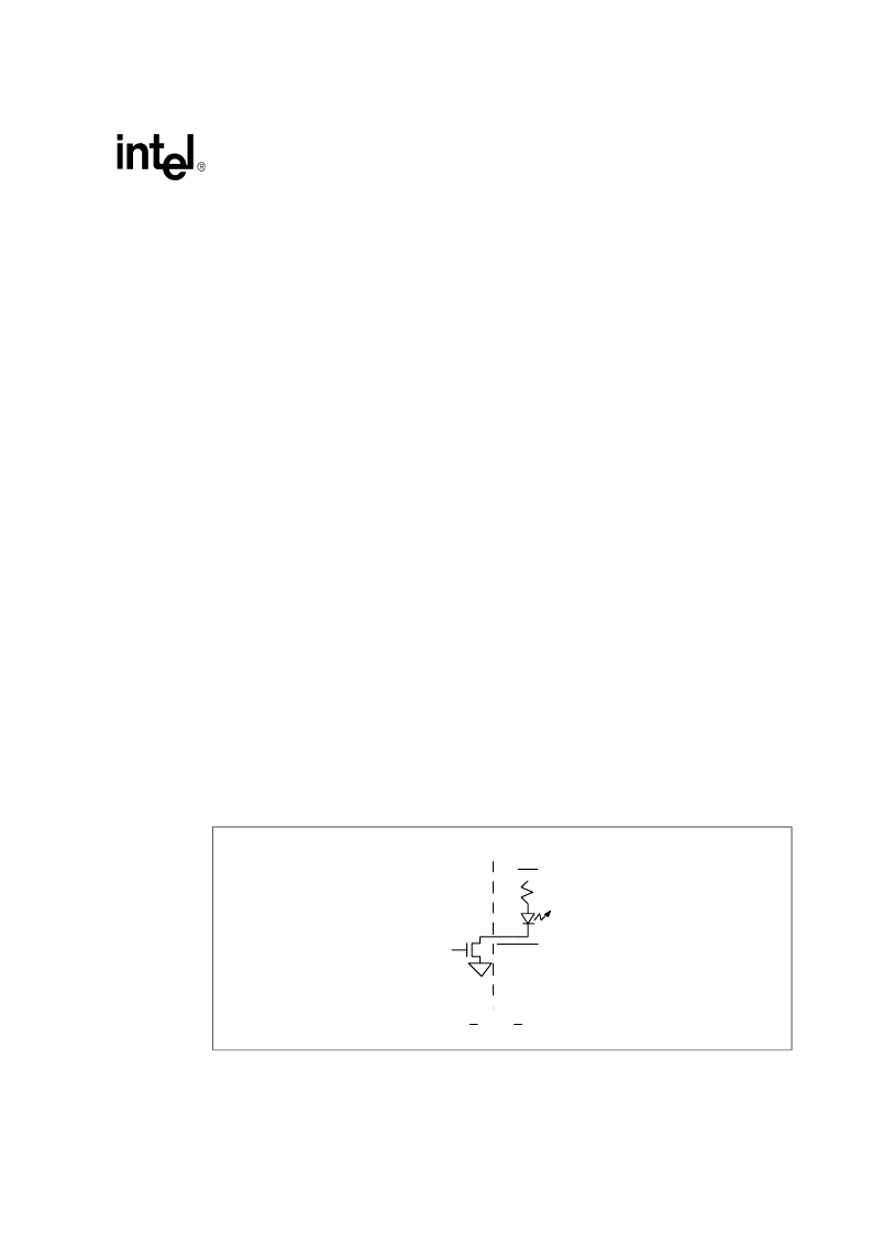
LED Circuit
Each Direct Drive LED has a corresponding open-drain pin. The LEDs are connected through a
current-limiting resistor to a positive-voltage rail. The LEDs are turned on when the output pin
drives Low. The open-drain LED pins are 5 V tolerant, allowing use of either a 3.3 V or 5 V rail (a
2.5 V rail is unlikely to work with standard forward voltage LEDs). A 5 V rail eases LED
component selection by allowing more common, high-forward voltage LEDs to be used. Refer to
Figure 33
for a circuit illustration.
Figure 33. LED Circuit
R
V
LED
Inside
IC
Outside
IC
LED
n
_m
VCCIO < V
LED
< 5 V + 5%
相關(guān)PDF資料 |
PDF描述 |
|---|---|
| DJIXELCD0QE001 | Advanced 8-Port 10/100 Mbps PHY Transceivers |
| DJIXELCD0SE000 | Advanced 8-Port 10/100 Mbps PHY Transceivers |
| DJIXELCD0SE001 | Advanced 8-Port 10/100 Mbps PHY Transceivers |
| DJIXELED0QE000 | Advanced 8-Port 10/100 Mbps PHY Transceivers |
| DJIXELED0QE001 | Advanced 8-Port 10/100 Mbps PHY Transceivers |
相關(guān)代理商/技術(shù)參數(shù) |
參數(shù)描述 |
|---|---|
| DJIXELCD0QE000 | 制造商:INTEL 制造商全稱:Intel Corporation 功能描述:Advanced 8-Port 10/100 Mbps PHY Transceivers |
| DJIXELCD0QE001 | 制造商:INTEL 制造商全稱:Intel Corporation 功能描述:Advanced 8-Port 10/100 Mbps PHY Transceivers |
| DJIXELCD0SE000 | 制造商:INTEL 制造商全稱:Intel Corporation 功能描述:Advanced 8-Port 10/100 Mbps PHY Transceivers |
| DJIXELCD0SE001 | 制造商:INTEL 制造商全稱:Intel Corporation 功能描述:Advanced 8-Port 10/100 Mbps PHY Transceivers |
| DJIXELED0QE000 | 制造商:INTEL 制造商全稱:Intel Corporation 功能描述:Advanced 8-Port 10/100 Mbps PHY Transceivers |
發(fā)布緊急采購,3分鐘左右您將得到回復(fù)。