- 您現(xiàn)在的位置:買賣IC網(wǎng) > PDF目錄223637 > CY2308 (Cypress Semiconductor Corp.) 3.3V Zero Delay Buffer PDF資料下載
參數(shù)資料
| 型號(hào): | CY2308 |
| 廠商: | Cypress Semiconductor Corp. |
| 英文描述: | 3.3V Zero Delay Buffer |
| 中文描述: | 3.3零延遲緩沖器 |
| 文件頁數(shù): | 8/14頁 |
| 文件大小: | 203K |
| 代理商: | CY2308 |
CY2308
Document #: 38-07146 Rev. *C
Page 3 of 14
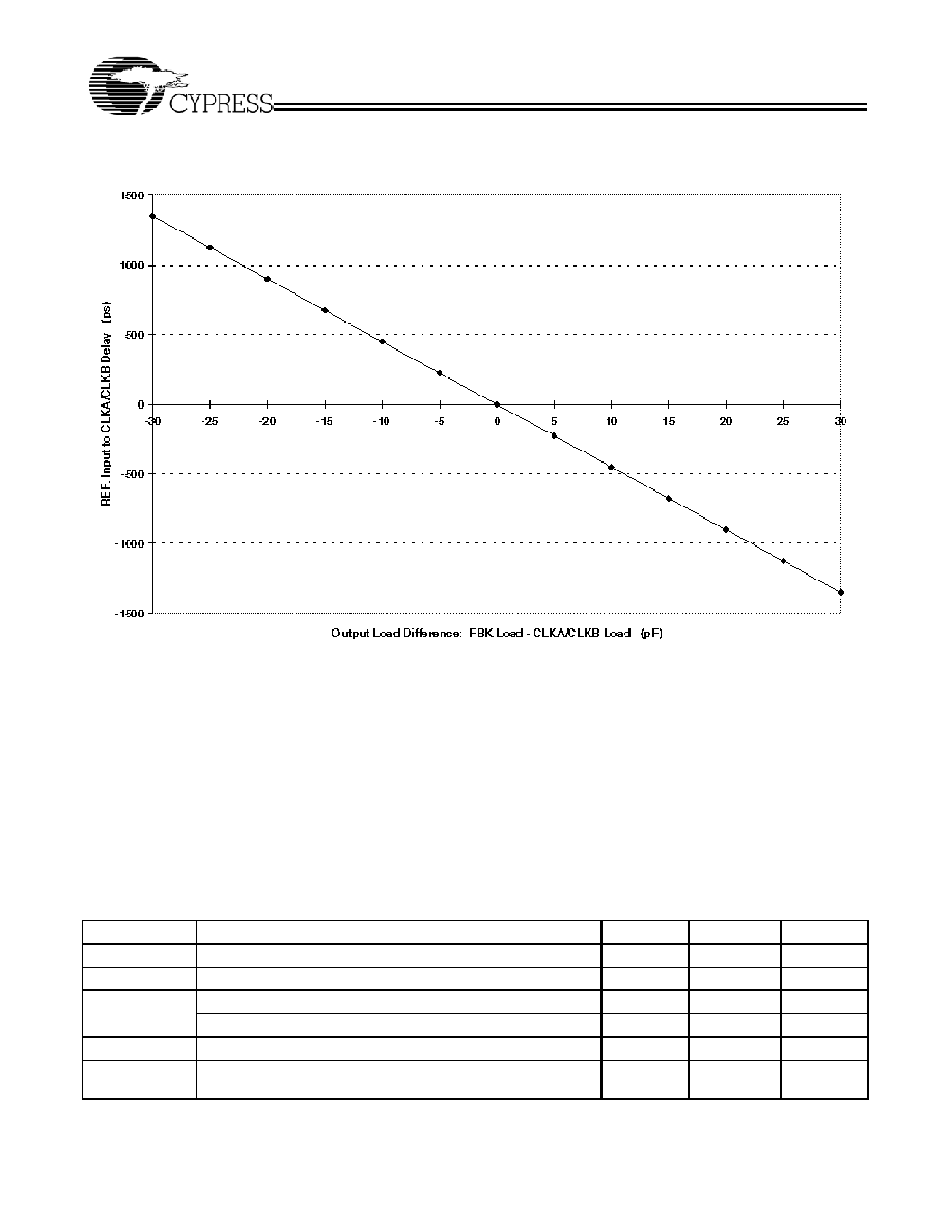
Zero Delay and Skew Control
To close the feedback loop of the CY2308, the FBK pin can be
driven from any of the eight available output pins. The output
driving the FBK pin will be driving a total load of 7 pF plus any
additional load that it drives. The relative loading of this output
(with respect to the remaining outputs) can adjust the input-
output delay. This is shown in the graph above.
For applications requiring zero input-output delay, all outputs
including the one providing feedback should be equally
loaded. If input-output delay adjustments are required, use the
above graph to calculate loading differences between the
feedback output and remaining outputs.
For zero output-output skew, be sure to load outputs equally.
For further information on using CY2308, refer to the appli-
cation note “CY2308: Zero Delay Buffer.”
Maximum Ratings
Supply Voltage to Ground Potential ...............–0.5V to +7.0V
DC Input Voltage (Except Ref) .............. –0.5V to VDD + 0.5V
DC Input Voltage REF ........................................... –0.5 to 7V
Storage Temperature.................................. –65°C to +150°C
Junction Temperature...................................................150°C
Static Discharge Voltage
(per MIL-STD-883, Method 3015) ............................. >2000V
REF. Input to CLKA/CLKB Delay v/s Difference in Loading between FBK pin and CLKA/CLKB Pins
Operating Conditions for CY2308SC-XX Commercial Temperature Devices
Parameter
Description
Min.
Max.
Unit
VDD
Supply Voltage
3.0
3.6
V
TA
Operating Temperature (Ambient Temperature)
0
70
°C
CL
Load Capacitance, below 100 MHz
30
pF
Load Capacitance, from 100 MHz to 133 MHz
15
pF
CIN
Input Capacitance[6]
7pF
tPU
Power-up time for all VDDs to reach minimum specified voltage
(power ramps must be monotonic)
0.05
50
ms
Note:
6. Applies to both Ref Clock and FBK.
相關(guān)PDF資料 |
PDF描述 |
|---|---|
| CY2309AZI-1H | 2309 SERIES, PLL BASED CLOCK DRIVER, 9 TRUE OUTPUT(S), 0 INVERTED OUTPUT(S), PDSO16 |
| CY23S09SXC-1T | 23S SERIES, PLL BASED CLOCK DRIVER, 8 TRUE OUTPUT(S), 0 INVERTED OUTPUT(S), PDSO16 |
| CY2DP818ZXCT | 2DP SERIES, LOW SKEW CLOCK DRIVER, 8 TRUE OUTPUT(S), 0 INVERTED OUTPUT(S), PDSO38 |
| CY2SSTV857LFC-32 | SSTV SERIES, PLL BASED CLOCK DRIVER, 10 TRUE OUTPUT(S), 0 INVERTED OUTPUT(S), QCC40 |
| CY2SSTV857LFXC-32T | SSTV SERIES, PLL BASED CLOCK DRIVER, 10 TRUE OUTPUT(S), 0 INVERTED OUTPUT(S), QCC40 |
相關(guān)代理商/技術(shù)參數(shù) |
參數(shù)描述 |
|---|---|
| CY2308_07 | 制造商:CYPRESS 制造商全稱:Cypress Semiconductor 功能描述:3.3V Zero Delay Buffer |
| CY2308_08 | 制造商:CYPRESS 制造商全稱:Cypress Semiconductor 功能描述:3.3V Zero Delay Buffer |
| CY2308_09 | 制造商:CYPRESS 制造商全稱:Cypress Semiconductor 功能描述:3.3V Zero Delay Buffer |
| CY2308_12 | 制造商:CYPRESS 制造商全稱:Cypress Semiconductor 功能描述:3.3 V Zero Delay Buffer |
| CY2308-1 | 制造商:CYPRESS 制造商全稱:Cypress Semiconductor 功能描述:3.3V Zero Delay Buffer |
發(fā)布緊急采購,3分鐘左右您將得到回復(fù)。