- 您現(xiàn)在的位置:買賣IC網(wǎng) > PDF目錄379830 > CDC2509PW (Texas Instruments, Inc.) 3.3-V PHASE-LOCK LOOP CLOCK DRIVER PDF資料下載
參數(shù)資料
| 型號: | CDC2509PW |
| 廠商: | Texas Instruments, Inc. |
| 英文描述: | 3.3-V PHASE-LOCK LOOP CLOCK DRIVER |
| 中文描述: | 3.3 - V相位鎖相環(huán)時鐘驅(qū)動器 |
| 文件頁數(shù): | 3/9頁 |
| 文件大?。?/td> | 132K |
| 代理商: | CDC2509PW |

CDC2509
3.3-V PHASE-LOCK LOOP CLOCK DRIVER
SCAS580A – OCTOBER 1996 – REVISED JANUARY 1998
3
POST OFFICE BOX 655303
DALLAS, TEXAS 75265
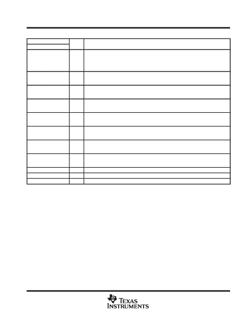
Terminal Functions
TERMINAL
TYPE
DESCRIPTION
NAME
NO.
CLK
24
I
Clock input. CLK provides the clock signal to be distributed by the CDC2509 clock driver. CLK is used
to provide the reference signal to the integrated PLL that generates the clock output signals. CLK must
have a fixed frequency and fixed phase for the PLL to obtain phase lock. Once the circuit is powered
up and a valid CLK signal is applied, a stabilization time is required for the PLL to phase lock the
feedback signal to its reference signal.
FBIN
13
I
Feedback input. FBIN provides the feedback signal to the internal PLL. FBIN must be hard-wired to
FBOUT to complete the PLL. The integrated PLL synchronizes CLK and FBIN so that there is
nominally zero phase error between CLK and FBIN.
1G
11
I
Output bank enable. 1G is the output enable for outputs 1Y(0:4). When 1G is low, outputs 1Y(0:4) are
disabled to a logic-low state. When 1G is high, all outputs 1Y(0:4) are enabled and switch at the same
frequency as CLK.
2G
14
I
Output bank enable. 2G is the output enable for outputs 2Y(0:3). When 2G is low, outputs 2Y(0:3) are
disabled to a logic low state. When 2G is high, all outputs 2Y(0:3) are enabled and switch at the same
frequency as CLK.
FBOUT
12
O
Feedback output. FBOUT is dedicated for external feedback. It switches at the same frequency as
CLK. When externally wired to FBIN, FBOUT completes the feedback loop of the PLL. FBOUT has
and integrated 25-
series-damping resistor.
Clock outputs. These outputs provide low-skew copies of CLK. Output bank 1Y(0:4) is enabled via
the 1G input. These outputs can be disabled to a logic-low state by deasserting the 1G control input.
Each output has an integrated 25-
series-damping resistor.
Clock outputs. These outputs provide low-skew copies of CLK. Output bank 2Y(0:3) is enabled via
the 2G input. These outputs can be disabled to a logic-low state by deasserting the 2G control input.
Each output has an integrated 25-
series-damping resistor.
Analog power supply. AVCC provides the power reference for the analog circuitry. In addition, AVCC
can be used to bypass the PLL for test purposes. When AVCC is strapped to ground, PLL is bypassed
and CLK is buffered directly to the device outputs.
1Y (0:4)
3, 4, 5, 8, 9
O
2Y (0:3)
16, 17, 20, 21
O
AVCC
23
Power
AGND
1
Ground
Analog ground. AGND provides the ground reference for the analog circuitry.
VCC
GND
2, 10, 15, 22
Power
Power supply
6, 7, 18, 19
Ground
Ground
相關(guān)PDF資料 |
PDF描述 |
|---|---|
| CDC2510APWRG4 | 3.3-V PHASE-LOCK LOOP CLOCK DRIVER |
| CDC2510BPW | 3.3-V PHASE-LOCK LOOP CLOCK DRIVER |
| CDC2510PW | 3.3-V PHASE-LOCK LOOP CLOCK DRIVER |
| CDC2516DGG | 3.3-V PHASE-LOCK LOOP CLOCK DRIVER |
| CDC2587 | Octal Divided -by-2 Circuit/Clock Driver(3.3V鎖相環(huán)時鐘驅(qū)動器(三態(tài)輸出)) |
相關(guān)代理商/技術(shù)參數(shù) |
參數(shù)描述 |
|---|---|
| CDC2509PWLE | 制造商:未知廠家 制造商全稱:未知廠家 功能描述:Nine Distributed-Output Clock Driver |
| CDC2509PWR | 功能描述:時鐘驅(qū)動器及分配 3.3V Ph-Lock Loop Clock Driver RoHS:否 制造商:Micrel 乘法/除法因子:1:4 輸出類型:Differential 最大輸出頻率:4.2 GHz 電源電壓-最大: 電源電壓-最小:5 V 最大工作溫度:+ 85 C 封裝 / 箱體:SOIC-8 封裝:Reel |
| CDC2509PWRG4 | 功能描述:時鐘驅(qū)動器及分配 3.3V Ph-Lock Loop Clock Driver RoHS:否 制造商:Micrel 乘法/除法因子:1:4 輸出類型:Differential 最大輸出頻率:4.2 GHz 電源電壓-最大: 電源電壓-最小:5 V 最大工作溫度:+ 85 C 封裝 / 箱體:SOIC-8 封裝:Reel |
| CDC2510 | 制造商:TI 制造商全稱:Texas Instruments 功能描述:3.3-V PHASE-LOCK LOOP CLOCK DRIVER |
| CDC2510A | 制造商:未知廠家 制造商全稱:未知廠家 功能描述:3.3-V Phase-Lock Loop Clock Driver |
發(fā)布緊急采購,3分鐘左右您將得到回復。