- 您現(xiàn)在的位置:買賣IC網(wǎng) > PDF目錄379806 > CD40104BMS (Intersil Corporation) CMOS 4-Bit Bidirectional Universal Shift Register(CMOS 4位雙向通用移位寄存器) PDF資料下載
參數(shù)資料
| 型號(hào): | CD40104BMS |
| 廠商: | Intersil Corporation |
| 英文描述: | CMOS 4-Bit Bidirectional Universal Shift Register(CMOS 4位雙向通用移位寄存器) |
| 中文描述: | 的CMOS 4位雙向通用移位寄存器(的CMOS 4位雙向通用移位寄存器) |
| 文件頁數(shù): | 1/10頁 |
| 文件大小: | 129K |
| 代理商: | CD40104BMS |

7-1307
CAUTION: These devices are sensitive to electrostatic discharge; follow proper IC Handling Procedures.
1-888-INTERSIL or 321-724-7143 | Copyright Intersil Corporation 1999
CD40104BMS,
CD40194BMS
CMOS 4-Bit Bidirectional
Universal Shift Register
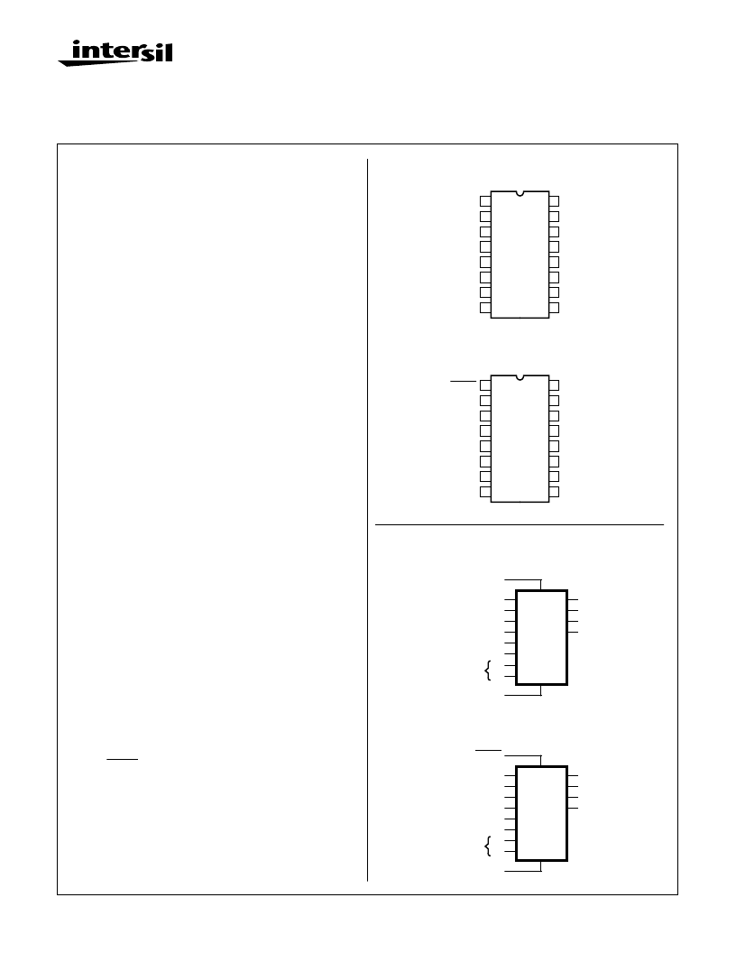
Pinouts
CD40104BMS
TOP VIEW
CD40194BMS
TOP VIEW
Functional Diagrams
CD40104BMS
CD40194BMS
14
15
16
9
13
12
11
10
1
2
3
4
5
7
6
8
OUTPUT ENABLE
SHIFT RIGHT IN
D0
D1
D2
D3
VSS
SHIFT LEVEL IN
VDD
Q1
Q2
Q3
CLOCK
SELECT 1
SELECT 0
Q0
14
15
16
9
13
12
11
10
1
2
3
4
5
7
6
8
RESET
SHIFT RIGHT IN
D0
D1
D2
D3
VSS
SHIFT LEVEL IN
VDD
Q1
Q2
Q3
CLOCK
SELECT 1
SELECT 0
Q0
3
4
5
6
7
2
9
10
D0
D1
D2
D3
CLOCK
S0
S1
SHIFT LEFT IN
SHIFT RIGHT IN
MODE SELECT
11
15
14
13
12
Q0
Q1
Q2
Q3
OUTPUT ENABLE
1
VDD = 16
VSS = 8
3
4
5
6
7
2
9
10
D0
D1
D2
D3
CLOCK
S0
S1
SHIFT LEFT IN
SHIFT RIGHT IN
MODE SELECT
11
15
14
13
12
Q0
Q1
Q2
Q3
RESET
1
VDD = 16
VSS = 8
Features
High Voltage Type (20V Rating)
Medium Speed fCL = 12MHz (typ.) at VDD = 10V
Fully Static Operation
Synchronous Parallel or Serial Operation
Three State Outputs (CD40104BMS)
Asynchronous Master Reset (CD40194BMS)
5V, 10V and 15V Parametric Ratings
Standardized Symmetrical Output Characteristics
Meets All Requirements of JEDEC Tentative Standard
No. 13B, “Standard Specifications for Description of
‘B’ Series CMOS Devices”
Applications
Arithmetic Unit Bus Registers
Serial/Parallel Conversions
General Purpose Register for Bus Organized Systems
General Purpose Registers
Description
The CD40104BMS is a universal shift register featuring parallel
inputs, parallel outputs, SHIFT RIGHT and SHIFT LEFT serial
inputs, and a high impedance third output state allowing the device
to be used in bus organized systems.
In the parallel load mode (S0 and S1 are high), data is loaded into
the associated flip-flop and appears at the output after the positive
transition of the CLOCK input. During loading, serial data flow is
inhibited. Shift right and shift left are accomplished synchronously
on the positive clock edge with serial data entered at the SHIFT
RIGHT and SHIFT LEFT serial inputs, respectively. Clearing the
register is accomplished by setting both mode controls low and
clocking the register. When the output enable input is low, all outputs
assume the high impedance state.
The CD40194BMS is a universal shift register featuring parallel inputs,
parallel outputs SHIFT RIGHT and SHIFT LEFT serial inputs, and a
direct overriding clear input. In the parallel load mode (S0 and S1 are
high), data is loaded into the associated flip-flop and appears at the out-
put after the positive transition of the CLOCK input. During loading,
serial data flow is inhibited. Shift right and shift left are accomplished
synchronously on the positive clock edge with data entered at the
SHIFT RIGHT and SHIFT LEFT serial inputs, respectively. Clocking of
the register is inhibited when both mode control inputs are low. When
low, the RESET input resets all stages and forces all outputs low. The
CD40194BMS is similar to industry types 340194 and MC40194.
The CD40104BMS and CD40194BMS series types are supplied in
these 16 lead outline packages
Braze Seal DIP
Frit Seal DIP
Ceramic Flatpack
* CD40104B Only
*HNX,
*H1L,
H6W
CD40194B Only
H4W
HIF
File Number
3352
December 1992
相關(guān)PDF資料 |
PDF描述 |
|---|---|
| CD40194BMS | CMOS 4-Bit Bidirectional Universal Shift Register |
| CD40105 | CMOS FIFO Register |
| CD40105BMS | CMOS FIFO Register(CMOS 先進(jìn)先出寄存器) |
| CD40106BC | Hex Schmitt Trigger(六施密特觸發(fā)器) |
| CD40106BMJ | 16-Bit Transparent D-Type Latch With 3-State Outputs 48-SSOP -40 to 85 |
相關(guān)代理商/技術(shù)參數(shù) |
參數(shù)描述 |
|---|---|
| CD40105 | 制造商:INTERSIL 制造商全稱:Intersil Corporation 功能描述:CMOS FIFO Register |
| CD40105B | 制造商:TI 制造商全稱:Texas Instruments 功能描述:CMOS FIFO REGISTER |
| CD40105BD | 制造商:Rochester Electronics LLC 功能描述:- Bulk |
| CD40105BDMSR | 制造商:Intersil Corporation 功能描述:FIFO REGISTER SGL 4-CH CMOS 16CDIP - Rail/Tube |
| CD40105BE | 功能描述:寄存器 CMOS FIFO RoHS:否 制造商:NXP Semiconductors 邏輯類型:CMOS 邏輯系列:HC 電路數(shù)量:1 最大時(shí)鐘頻率:36 MHz 傳播延遲時(shí)間: 高電平輸出電流:- 7.8 mA 低電平輸出電流:7.8 mA 電源電壓-最大:6 V 最大工作溫度:+ 125 C 封裝 / 箱體:SOT-38 封裝:Tube |
發(fā)布緊急采購,3分鐘左右您將得到回復(fù)。