- 您現(xiàn)在的位置:買賣IC網(wǎng) > PDF目錄1904 > ATAM893T-TKSYD (Atmel)IC MCU FLASH 4K MTP 20SSOP PDF資料下載
第1頁第2頁第3頁第4頁第5頁第6頁第7頁第8頁第9頁第10頁第11頁第12頁第13頁第14頁第15頁第16頁第17頁第18頁第19頁第20頁第21頁第22頁第23頁第24頁第25頁第26頁第27頁第28頁第29頁第30頁第31頁第32頁第33頁第34頁第35頁第36頁第37頁第38頁第39頁第40頁第41頁當(dāng)前第42頁第43頁第44頁第45頁第46頁第47頁第48頁第49頁第50頁第51頁第52頁第53頁第54頁第55頁第56頁第57頁第58頁第59頁第60頁第61頁第62頁第63頁第64頁第65頁第66頁第67頁第68頁第69頁第70頁第71頁第72頁第73頁第74頁第75頁第76頁第77頁第78頁第79頁第80頁第81頁第82頁第83頁第84頁第85頁第86頁第87頁第88頁第89頁第90頁第91頁第92頁第93頁第94頁第95頁第96頁第97頁第98頁
47
4680C–4BMCU–01/05
ATAM893-D
5.3.3
Timer 3
5.3.3.1
Features
Two Compare Registers
Capture Register
Edge Sensitive Input with Zero Cross Detection Capability
Trigger and Single Action Modes
Output Control Modes
Automatic Modulation and Demodulation Modes
FSK Modulation
Pulse width Modulation (PWM)
Manchester Demodulation Together with SSI
Bi-phase Demodulation Together with SSI
Pulse-width Demodulation Together with SSI
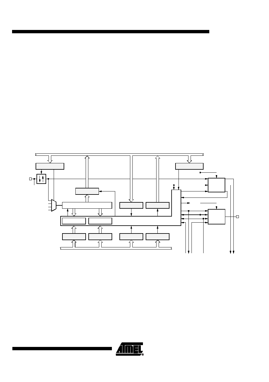
Figure 5-24. Timer 3
Timer 3 consists of an 8-bit up-counter with two compare registers and one capture register. The
timer can be used as event counter, timer and signal generator. Its output can be programmed
as modulator and demodulator for the serial interface. The two compare registers enable various
modes of signal generation, modulation and demodulation. The counter can be driven by inter-
nal and external clock sources. For external clock sources, it has a programmable edge-
sensitive input which can be used as counter input, capture signal input or trigger input. This
timer input is synchronized with SYSCL. Therefore, in the power-down mode SLEEP (CPU core
→sleep and OSC-Stop →yes), this timer input is stopped too. The counter is readable via its
capture register while it is running. In capture mode, the counter value can be captured by a pro-
grammable capture event from the Timer 3 input or Timer 2 output.
8-bit Counter 3
RES
Compare 3/1
T3CO1
T3CP
T3CO2
Control
T3O
CL3
T3I
T3EX
SYSCL
T1OUT
POUT
I/O-bus
Compare 3/2
T3CM1
T3CM2
T3C
T3ST
Modulator 3
Demodu-
lator 3
M2
Control
SO
TOG3
INT5
RES
CM31
T3I
T3EX
TOG2
SI
SCI
T3M
T3CS
I/O-bus
Timer 2
SSI
CP3
相關(guān)PDF資料 |
PDF描述 |
|---|---|
| ATF1500ABV-15JI | IC CPLD 15NS LOW VOLT PLCC |
| ATF1500AL-20JI | IC CPLD 20NS LOW POW 44PLCC |
| ATF1502ASV-15JI44 | IC CPLD EE HP 15NS 44-PLCC |
| ATF1502BE-5AX44 | IC CPLD 64MC 1.8V 44-TQFP |
| ATF1504ASVL-20QI100 | IC CPLD 20NS LOWV LOWPWR 100QPFP |
相關(guān)代理商/技術(shù)參數(shù) |
參數(shù)描述 |
|---|---|
| ATAM893X-TKHYZ | 制造商:ATMEL 制造商全稱:ATMEL Corporation 功能描述:Flash Version for ATAR080, ATAR090/890 and ATAR092/892 |
| ATAM893X-TKQYZ | 制造商:ATMEL 制造商全稱:ATMEL Corporation 功能描述:Flash Version for ATAR080, ATAR090/890 and ATAR092/892 |
| ATAM893X-TKSYZ | 制造商:ATMEL 制造商全稱:ATMEL Corporation 功能描述:Flash Version for ATAR080, ATAR090/890 and ATAR092/892 |
| ATAM894 | 制造商:ATMEL 制造商全稱:ATMEL Corporation 功能描述:8k-flash Microcontroller |
| ATAM894P | 制造商:ATMEL 制造商全稱:ATMEL Corporation 功能描述:MARC4 4-bit Microcontrollers |
發(fā)布緊急采購,3分鐘左右您將得到回復(fù)。