- 您現(xiàn)在的位置:買賣IC網(wǎng) > PDF目錄375315 > AN10145 (NXP Semiconductors N.V.) Bi-directional low voltage translators PDF資料下載
參數(shù)資料
| 型號(hào): | AN10145 |
| 廠商: | NXP Semiconductors N.V. |
| 英文描述: | Bi-directional low voltage translators |
| 中文描述: | 雙向低電壓轉(zhuǎn)換器 |
| 文件頁數(shù): | 20/24頁 |
| 文件大?。?/td> | 325K |
| 代理商: | AN10145 |
20
Answer::
The low voltage limit is not in the DC specifications but the bullet under "Features" states level
translation down to 1 V. The GTL20xx devices SREF is not recommended below 1 V to insure a low on resistance.
The problem with a SREF voltage lower than 1V is that the gate overdrive, or the amount that the gate voltage is
above the threshold, decreases as the SREF voltage is lowered. This means that the NMOS transistor does not turn
on as hard and so the on resistance increases. Once you get below a certain gate overdrive, the on resistance
increases rapidly. The part will still be functional, but the on resistance will be higher.
10.
Question
: We want to use the GTL2010 to translate signals from 1.5 V to 3.3 V so our settings will be V
SREF
=
1.5V, V
DREF
= 3.3V. But we use only 6-bits of the 10-bit GTL2010, so there are 4-bits unused. We plan to use these
other 4-bits for signal translation from 3.3V to 5V. Looking through the application note we know that if the V
DREF
is changed to 5V, then the GTL2010 can support both 3.3V and 5V output mix on the D side. But is it suitable for
V
SREF
to be changed to 3.3V so that the input will support both a 1.5V and 3.3V input mix on the S side
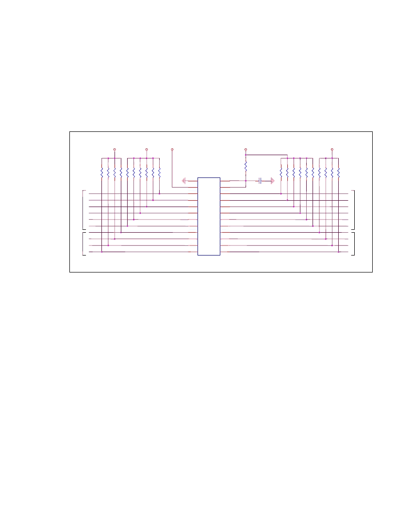
Figure 18. Application Diagram
Answer:
To protect the 1.5 V parts the SREF must stay at 1.5 V and you will have to rely on the 3.3 V pull-up on
the S side and the 5 V pull-up on the D side to get the high levels since the path will be essentially cut off above 1.5
V. It is possible to mix the voltages as proposed but the SREF must be 1.5 V and the resistors on both the 3.3 V and
5 V sides determine the highs with the low being passed through the GTL2010.
11.
Multi-part Question:
I have a design where I need to translate voltage levels. My design needs fix 3.3V levels on D side.
Voltage levels on S side vary from 1.8V to 5V. So I did the following:
1. SREF to 1.8 V, GREF+DREF through R = 200 k
to 5 V, D pins pull-ups to 3.3 V. This is 1.8 V compliant on
S side.
2. SREF to 3.3 V, GREF+DREF through R = 200 k
to 5 V, D pins pull-ups to 3.3 V. This is 3.3 V compliant on
S side.
3. SREF+GREF through R=200 k
to 5 V, DREF to 3.3 V, D pins pull-ups to 3.3 V. S pins pull-up to 5 V. I
assume that DREF pin is now Vreference so it should not exceed 4.4V and should be 1.5 V below GREF. This
is 5.0 V compliant on S side. The level on D side is 3.3 V.
Question A:
Am I right for the last assumption and is my design correct
Answer A:
We assume that you are describing three different parts or at least three different jumper
configurations, that is the 1.8 V, 3.3 V, and 5 V are not all present on different sources and drains at the same
time because the level shift can only be down to one low voltage level per part/configuration.
The answer to 3 is yes, the S and D are labels, the electrical characteristics are identical so connecting the SREF
and GREF together and using a 200 k
resistor to 5 V to bias them with the DREF at 3.3 V is equivalent to
connecting the DREF and GREF together and biasing them through the 200 K ohm resistor to 5 V, with the
R
R
C1
0.1uF
5V
1.5V
R
R
R
3.3V
signa
U1
GTL2010
1
24
2
23
22
21
20
19
18
17
16
15
14
13
3
4
5
6
7
8
9
10
11
12
GND
Gref
Sref
Dref
D1
D2
D3
D4
D5
D6
D7
D8
D9
D10
S1
S2
S3
S4
S5
S6
S7
S8
S9
S10
5V
signa
1.5V
signal
R
R
3.3V
signal
R
R
R
3.3V
3.3V
R
R
R
R
R
3.3V
R
R
R
R1
R
R
相關(guān)PDF資料 |
PDF描述 |
|---|---|
| AN101 | Circular Connector; No. of Contacts:3; Series:MS27508; Body Material:Aluminum; Connecting Termination:Crimp; Connector Shell Size:8; Circular Contact Gender:Pin; Circular Shell Style:Box Mount Receptacle; Insert Arrangement:8-98 RoHS Compliant: No |
| AN104 | AN104 |
| AN105 | FETS AS VOLTAGE-CONTROLLED RESISTORS |
| AN1201SM | Polarity inverting charge pump DC/DC converter IC |
| AN1324 | Circular Connector; No. of Contacts:4; Series:MS27508; Body Material:Aluminum; Connecting Termination:Crimp; Connector Shell Size:8; Circular Contact Gender:Socket; Circular Shell Style:Box Mount Receptacle; Insert Arrangement:8-44 RoHS Compliant: No |
相關(guān)代理商/技術(shù)參數(shù) |
參數(shù)描述 |
|---|---|
| AN1016/D | 制造商:未知廠家 制造商全稱:未知廠家 功能描述:Infrared Sensing and Data Transmission Fundamentals |
| AN101-N01 | 制造商:SMC Corporation of America 功能描述:Silencer, pneumatic, general purpose,1/8in. NPT thread, 16dB |
| AN10-20A | 制造商:AN# - MILITARY 功能描述: |
| AN102101 | 制造商:The Cherry Corporation 功能描述:ONE-PIECE ANGULAR POSITION SENSOR 制造商:CHERRY ELECTRICAL PRODUCTS 功能描述:ONE-PIECE ANGULAR POSITION SENSOR 制造商:Cherry 功能描述:ONE-PIECE ANGULAR POSITION SENSOR |
| AN1025 | 制造商:MICROCHIP 制造商全稱:Microchip Technology 功能描述:Converting A 5.0V Supply Rail To A Regulated 3.0V |
發(fā)布緊急采購,3分鐘左右您將得到回復(fù)。