- 您現(xiàn)在的位置:買賣IC網(wǎng) > PDF目錄375310 > AM70PDL129BDH85IS (SPANSION LLC) 2 x 64 Megabit (8 M x 16-Bit) CMOS 3.0 Volt-Only Page Mode Flash Memory Data Storage 128 Megabit (8 M x 16-Bit) CMOS PDF資料下載
參數(shù)資料
| 型號: | AM70PDL129BDH85IS |
| 廠商: | SPANSION LLC |
| 元件分類: | 存儲器 |
| 英文描述: | 2 x 64 Megabit (8 M x 16-Bit) CMOS 3.0 Volt-Only Page Mode Flash Memory Data Storage 128 Megabit (8 M x 16-Bit) CMOS |
| 中文描述: | SPECIALTY MEMORY CIRCUIT, PBGA93 |
| 封裝: | 13 X 9 MM, FBGA-93 |
| 文件頁數(shù): | 60/128頁 |
| 文件大小: | 918K |
| 代理商: | AM70PDL129BDH85IS |
第1頁第2頁第3頁第4頁第5頁第6頁第7頁第8頁第9頁第10頁第11頁第12頁第13頁第14頁第15頁第16頁第17頁第18頁第19頁第20頁第21頁第22頁第23頁第24頁第25頁第26頁第27頁第28頁第29頁第30頁第31頁第32頁第33頁第34頁第35頁第36頁第37頁第38頁第39頁第40頁第41頁第42頁第43頁第44頁第45頁第46頁第47頁第48頁第49頁第50頁第51頁第52頁第53頁第54頁第55頁第56頁第57頁第58頁第59頁當前第60頁第61頁第62頁第63頁第64頁第65頁第66頁第67頁第68頁第69頁第70頁第71頁第72頁第73頁第74頁第75頁第76頁第77頁第78頁第79頁第80頁第81頁第82頁第83頁第84頁第85頁第86頁第87頁第88頁第89頁第90頁第91頁第92頁第93頁第94頁第95頁第96頁第97頁第98頁第99頁第100頁第101頁第102頁第103頁第104頁第105頁第106頁第107頁第108頁第109頁第110頁第111頁第112頁第113頁第114頁第115頁第116頁第117頁第118頁第119頁第120頁第121頁第122頁第123頁第124頁第125頁第126頁第127頁第128頁
58
Am70PDL127BDH/Am70PDL129BDH
November 25, 2003
A D V A N C E I N F O R M A T I O N
ABSOLUTE MAXIMUM RATINGS
Storage Temperature
Plastic Packages . . . . . . . . . . . . . . . –55
°
C to +125
°
C
Ambient Temperature
with Power Applied. . . . . . . . . . . . . . . –40
°
C to +85
°
C
Voltage with Respect to Ground
V
CC
f, V
CC
s (Note 1). . . . . . . . . . . .–0.5 V to +4.0 V
RESET# (Note 2) . . . . . . . . . . . .–0.5 V to +12.5 V
WP#/ACC . . . . . . . . . . . . . . . . . .–0.5 V to +10.5 V
All other pins (Note 1). . . . . . –0.5 V to V
CC
+0.5 V
Output Short Circuit Current (Note 3) . . . . . . 200 mA
Notes:
1. Minimum DC voltage on input or I/O pins is –0.5 V
During voltage transitions, input or I/O pins may
overshoot V
SS
to –2.0 V for periods of up to 20 ns.
Maximum DC voltage on input or I/O pins is V
CC
+0.5 V.
See Figure 8. During voltage transitions, input or I/O pins
may overshoot to V
CC
+2.0 V for periods up to 20 ns. See
Figure 9.
2. Minimum DC input voltage on pins RESET#, and
WP#/ACC is –0.5 V. During voltage transitions,
WP#/ACC, and RESET# may overshoot V
SS
to –2.0 V for
periods of up to 20 ns. See Figure 8. Maximum DC input
voltage on pin RESET# is +12.5 V which may overshoot
to +14.0 V for periods up to 20 ns. Maximum DC input
voltage on WP#/ACC is +9.5 V which may overshoot to
+12.0 V for periods up to 20 ns.
3. No more than one output may be shorted to ground at a
time. Duration of the short circuit should not be greater
than one second.
Stresses above those listed under “Absolute Maximum
Ratings” may cause permanent damage to the device. This
is a stress rating only; functional operation of the device at
these or any other conditions above those indicated in the
operational sections of this data sheet is not implied.
Exposure of the device to absolute maximum rating
conditions for extended periods may affect device reliability.
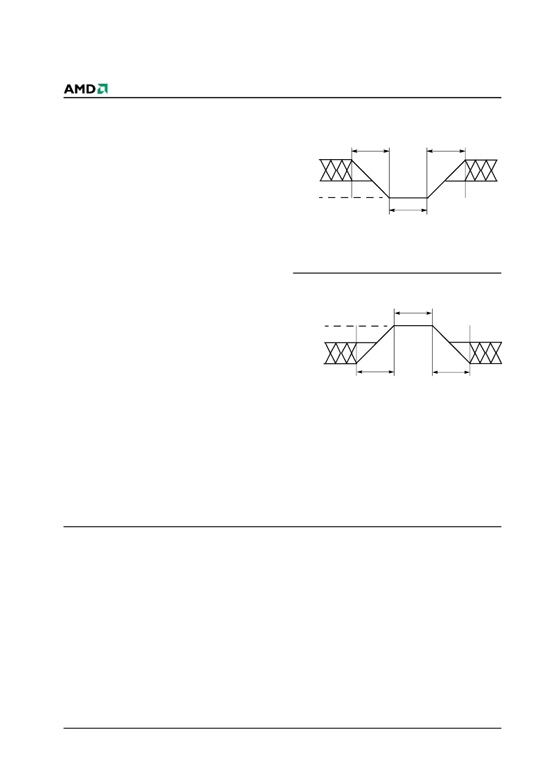
Figure 8.
Maximum Negative
Overshoot Waveform
Figure 9.
Overshoot Waveform
Maximum Positive
OPERATING RANGES
Industrial (I) Devices
Ambient Temperature (T
A
) . . . . . . . . . –40°C to +85°C
V
CC
f/V
CC
s Supply Voltages
V
CC
f/V
CC
s
for standard voltage range . .2.7 V to 3.3 V
Operating ranges define those limits between which the
functionality of the device is guaranteed.
20 ns
20 ns
+0.8 V
–0.5 V
20 ns
–2.0 V
20 ns
20 ns
V
+2.0 V
V
+0.5 V
20 ns
2.0 V
相關PDF資料 |
PDF描述 |
|---|---|
| AM70PDL129BDH85IT | 2 x 64 Megabit (8 M x 16-Bit) CMOS 3.0 Volt-Only Page Mode Flash Memory Data Storage 128 Megabit (8 M x 16-Bit) CMOS |
| AM70PDL127CDH | Stacked Multi-Chip Package (MCP/XIP) Flash Memory, Data storage MirrorBit Flash, and pSRAM (XIP) |
| AM70PDL127CDH66I | Stacked Multi-Chip Package (MCP/XIP) Flash Memory, Data storage MirrorBit Flash, and pSRAM (XIP) |
| AM70PDL127CDH66IS | Stacked Multi-Chip Package (MCP/XIP) Flash Memory, Data storage MirrorBit Flash, and pSRAM (XIP) |
| AM70PDL127CDH66IT | Stacked Multi-Chip Package (MCP/XIP) Flash Memory, Data storage MirrorBit Flash, and pSRAM (XIP) |
相關代理商/技術參數(shù) |
參數(shù)描述 |
|---|---|
| AM70PDL129BDH85IT | 制造商:SPANSION 制造商全稱:SPANSION 功能描述:2 x 64 Megabit (8 M x 16-Bit) CMOS 3.0 Volt-Only Page Mode Flash Memory Data Storage 128 Megabit (8 M x 16-Bit) CMOS |
| AM70PDL129CDH | 制造商:SPANSION 制造商全稱:SPANSION 功能描述:Stacked Multi-Chip Package (MCP/XIP) Flash Memory, Data storage MirrorBit Flash, and pSRAM (XIP) |
| AM70PDL129CDH66I | 制造商:SPANSION 制造商全稱:SPANSION 功能描述:Stacked Multi-Chip Package (MCP/XIP) Flash Memory, Data storage MirrorBit Flash, and pSRAM (XIP) |
| AM70PDL129CDH66IS | 制造商:SPANSION 制造商全稱:SPANSION 功能描述:Stacked Multi-Chip Package (MCP/XIP) Flash Memory, Data storage MirrorBit Flash, and pSRAM (XIP) |
| AM70PDL129CDH66IT | 制造商:SPANSION 制造商全稱:SPANSION 功能描述:Stacked Multi-Chip Package (MCP/XIP) Flash Memory, Data storage MirrorBit Flash, and pSRAM (XIP) |
發(fā)布緊急采購,3分鐘左右您將得到回復。