- 您現(xiàn)在的位置:買賣IC網(wǎng) > PDF目錄375269 > ADV7189KST (ANALOG DEVICES INC) Multiformat SDTV Video Decoder PDF資料下載
參數(shù)資料
| 型號: | ADV7189KST |
| 廠商: | ANALOG DEVICES INC |
| 元件分類: | 顏色信號轉(zhuǎn)換 |
| 英文描述: | Multiformat SDTV Video Decoder |
| 中文描述: | COLOR SIGNAL DECODER, PQFP80 |
| 封裝: | LEAD FREE, MS-026-BEC, LQFP-80 |
| 文件頁數(shù): | 63/104頁 |
| 文件大小: | 890K |
| 代理商: | ADV7189KST |
第1頁第2頁第3頁第4頁第5頁第6頁第7頁第8頁第9頁第10頁第11頁第12頁第13頁第14頁第15頁第16頁第17頁第18頁第19頁第20頁第21頁第22頁第23頁第24頁第25頁第26頁第27頁第28頁第29頁第30頁第31頁第32頁第33頁第34頁第35頁第36頁第37頁第38頁第39頁第40頁第41頁第42頁第43頁第44頁第45頁第46頁第47頁第48頁第49頁第50頁第51頁第52頁第53頁第54頁第55頁第56頁第57頁第58頁第59頁第60頁第61頁第62頁當(dāng)前第63頁第64頁第65頁第66頁第67頁第68頁第69頁第70頁第71頁第72頁第73頁第74頁第75頁第76頁第77頁第78頁第79頁第80頁第81頁第82頁第83頁第84頁第85頁第86頁第87頁第88頁第89頁第90頁第91頁第92頁第93頁第94頁第95頁第96頁第97頁第98頁第99頁第100頁第101頁第102頁第103頁第104頁
ADV7189
PIXEL PORT CONFIGURATION
The ADV7189 has a very flexible pixel port that can be config-
ured in a variety of formats to accommodate downstream ICs.
Table 168 and Table 169 summarize the various functions that
the ADV7189’s pins can have in different modes of operation.
Rev. A | Page 63 of 104
The ordering of components (e.g., Cr versus Cb, CHA/B/C) can
be changed. Refer to the SWPC Swap Pixel Cr/Cb (SDP),
Address 0x27, [7] section. Table 168 indicates the default
positions for the Cr/Cb components.
OF_SEL[3:0] Output Format Selection, Address 0x03, [5:2]
There are several modes in which the ADV7189 pixel port can
be configured. These modes are under the control of
OF_SEL[3:0]. See Table 169 for more details.
The default LLC frequency output on the LLC1 pin is approxi-
mately 27 MHz. For modes that operate with a nominal data
rate of 13.5 MHz (0001, 0010), the clock frequency on the LLC1
pin stays at the higher rate of 27 MHz. For information on
outputting the nominal 13.5 MHz clock on the LLC1 pin, see
the LLC1 Output Selection, LLC_PAD_SEL[2:0] (SDP),
Address 0x8F, [6:4] section.
SWPC Swap Pixel Cr/Cb (SDP), Address 0x27, [7]
This bit allows Cr and Cb samples of the SDP block to be
swapped.
Table 166. SWPC Function
SWPC
Description
0*
No swapping.
1
Swap Cr and Cb values.
*Default value.
LLC1 Output Selection, LLC_PAD_SEL[2:0] (SDP),
Address 0x8F, [6:4]
The following I
2
C write allows the user to select between the
LLC1 (nominally at 27 MHz) and LLC2 (nominally at
13.5 MHz).
The LLC2 signal is useful for LLC2 compatible wide bus
(16-/20-bit) output modes. See OF_SEL[3:0] for additional
information. The LLC2 signal and data on the data bus are
synchronized. By default, the rising edge of LLC1/LLC2 is
aligned with the Y data; the falling edge occurs when the data
bus holds C data. The polarity of the clock, and therefore the
Y/C assignments to the clock edges, can be altered by using the
Polarity LLC pin.
Table 167. LLC_PAD_SEL Function
LLC_PAD_SEL[2:0]
Description
000*
Output nominal 27 MHz LLC on LLC1 pin
101
Output nominal 13.5 MHz LLC on LLC1 pin
*Default value.
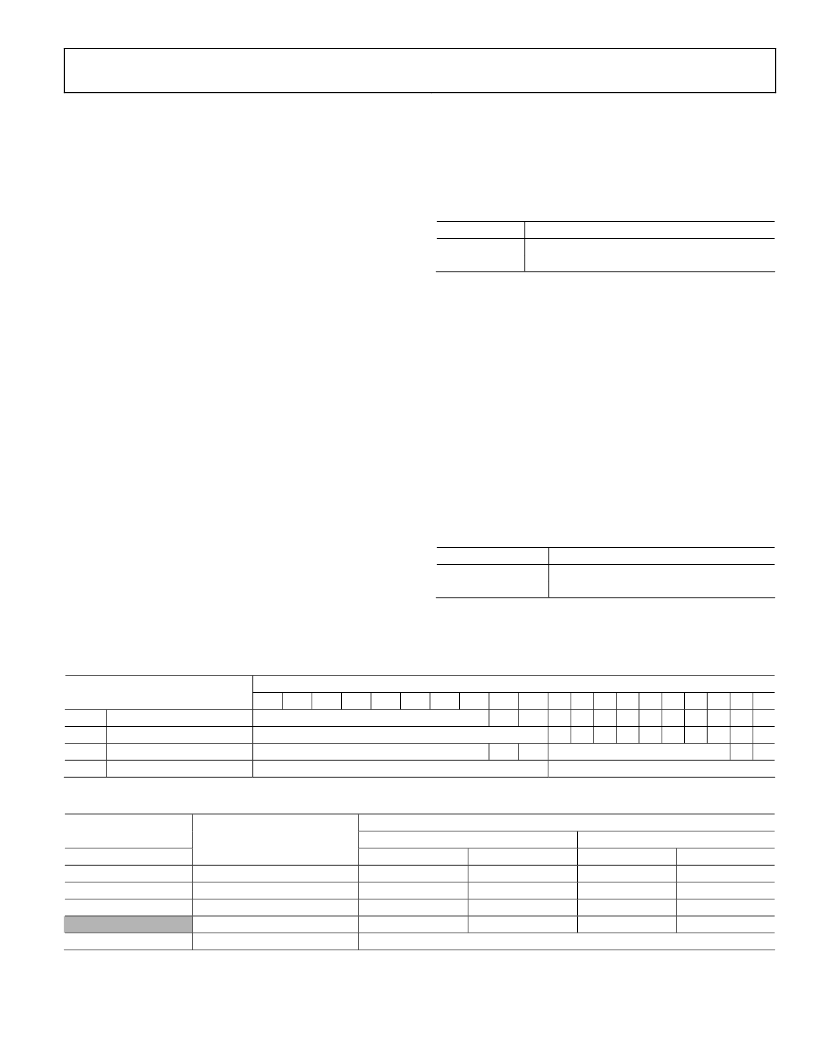
Table 168. P19–P0 Output/Input Pin Mapping
Data Port Pins P[19:0]
12
11
Processor, Format, and Mode
SDP
Video Out, 8-Bit, 4:2:2
SDP
Video Out, 10-Bit, 4:2:2
SDP
Video Out, 16-Bit, 4:2:2
SDP
Video Out, 20-Bit, 4:2:2
19
18
17
16
15
14
13
10
9
8
7
CrCb[7:0] OUT
CrCb[9:0] OUT
6
5
4
3
2
1
0
YCrCb[7:0]OUT
YCrCb[9:0]OUT
Y[7:0]OUT
Y[9:0]OUT
Table 169. Standard Definition Pixel Port Modes
Function
OF_SEL[3:0]
Format
0000
10-Bit @ LLC1 4:2:2
0001
20-Bit @ LLC2 4:2:2
0010
16-Bit @ LLC2 4:2:2
0011*
8-Bit @ LLC1 4:2:2
0110-1111
Reserved
*Default value.
Pixel Port Pins P[19:0]
P[19:10]
P9[9:0]
P[19:12]
YCrCb[9:2]
Y[9:2]
Y[7:0]
YCrCb[7:0]
P[11:10]
YCrCb[1:0]
Y[1:0]
Three-State
Three-State
P[9:2]
Three-State
CrCb[9:2]
CrCb[7:0]
Three-State
P[1:0]
Three-State
CrCb[1:0]
Three-State
Three-State
Reserved. Do not use.
相關(guān)PDF資料 |
PDF描述 |
|---|---|
| ADV7195 | Multiformat Progressive Scan/HDTV Encoder with Three 11-Bit DACs and 10-Bit Data Input |
| ADV7195KST | Multiformat Progressive Scan/HDTV Encoder with Three 11-Bit DACs and 10-Bit Data Input |
| ADV7196 | Multiformat Progressive Scan/HDTV Encoder with Three 11-Bit DACs, 10-Bit Data Input, and Macrovision |
| ADV7196A | Multiformat Progressive Scan/HDTV Encoder with Three 11-Bit DACs, 10-Bit Data Input, and Macrovision |
| ADV7196AKS | Multiformat Progressive Scan/HDTV Encoder with Three 11-Bit DACs, 10-Bit Data Input, and Macrovision |
相關(guān)代理商/技術(shù)參數(shù) |
參數(shù)描述 |
|---|---|
| ADV7189XST | 制造商:Analog Devices 功能描述:54MHZ NTSC/PAL ENCODER(DNR+MACROVISON)IC - Bulk |
| ADV7189XST-X2 | 制造商:Analog Devices 功能描述:54MHZ NTSC/PAL ENCODER(DNR+MACROVISON)IC - Bulk |
| ADV7190 | 制造商:Panasonic Industrial Company 功能描述:IC |
| ADV7190KST | 制造商:AD 制造商全稱:Analog Devices 功能描述:Video Encoder with Six 10-Bit DACs and Video Encoder with Six DAC Outputs |
| ADV7190KSTZ | 制造商:Analog Devices 功能描述:Video Encoder 6DAC 10-Bit 64-Pin LQFP |
發(fā)布緊急采購,3分鐘左右您將得到回復(fù)。