- 您現(xiàn)在的位置:買賣IC網(wǎng) > PDF目錄375269 > ADV7150LS220 (ANALOG DEVICES INC) CMOS 220 MHz True-Color Graphics Triple 10-Bit Video RAM-DAC PDF資料下載
參數(shù)資料
| 型號(hào): | ADV7150LS220 |
| 廠商: | ANALOG DEVICES INC |
| 元件分類: | 顯示控制器 |
| 英文描述: | CMOS 220 MHz True-Color Graphics Triple 10-Bit Video RAM-DAC |
| 中文描述: | PALETTE-DAC DSPL CTLR, PQFP160 |
| 封裝: | POWER, PLASTIC, QFP-160 |
| 文件頁數(shù): | 3/36頁 |
| 文件大小: | 447K |
| 代理商: | ADV7150LS220 |
第1頁第2頁當(dāng)前第3頁第4頁第5頁第6頁第7頁第8頁第9頁第10頁第11頁第12頁第13頁第14頁第15頁第16頁第17頁第18頁第19頁第20頁第21頁第22頁第23頁第24頁第25頁第26頁第27頁第28頁第29頁第30頁第31頁第32頁第33頁第34頁第35頁第36頁
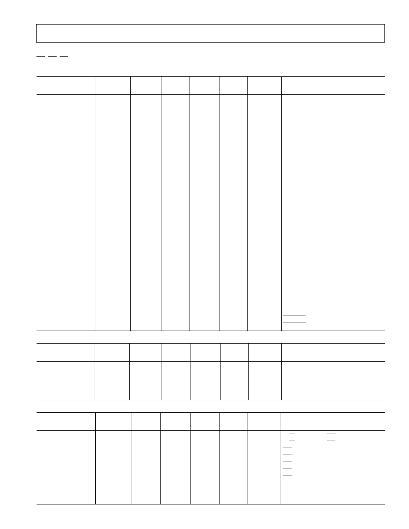
ADV7150
–3–
REV. A
TIMNGCHARACTERISTICS
1
IOR
,
IOG
,
I0B
= GND. All specifications T
MN
to T
MAX3
unless otherwse noted.)
CLOCK CONT ROL AND PIX E L PORT
4
220 MHz 170 MHz 135 MHz 110 MHz 85 MHz
Version
Version
Version
Parameter
Version
Version
Units
Conditions/Comments
f
CLOCK
t
1
t
2
t
3
t
4
f
LOADIN
1:1 Multiplexing
2:1 Multiplexing
4:1 Multiplexing
t
5
1:1 Multiplexing
2:1 Multiplexing
4:1 Multiplexing
t
6
1:1 Multiplexing
2:1 Multiplexing
4:1 Multiplexing
t
7
1:1 Multiplexing
2:1 Multiplexing
4:1 Multiplexing
t
8
t
9
t
10
τ
–t
115
t
PD6
1:1 Multiplexing
2:1 Multiplexing
4:1 Multiplexing
t
12
t
13
t
14
t
15
220
4.55
2
2
10
170
5.88
2.5
2.5
10
135
7.4
3.2
3
10
110
9.1
4
4
10
85
11.77
4
4
10
MHz max
ns min
ns min
ns min
ns max
Pixel CLOCK Rate
Pixel CLOCK Cycle T ime
Pixel CLOCK High T ime
Pixel CLOCK Low T ime
Pixel CLOCK to LOADOUT Delay
LOADIN Clocking Rate
110
110
55
110
85
42.5
110
67.5
33.75
110
55
27.5
85
42.5
21.25
MHz max
MHz max
MHz max
LOADIN Cycle T ime
9.1
9.1
18.18
9.1
11.76
23.53
9.1
14.8
29.63
9.1
18.18
36.36
9.1
23.53
47.1
ns min
ns min
ns min
LOADIN High T ime
4
4
8
4
5
9
4
6
12
4
8
15
4
9
18
ns min
ns min
ns min
LOADIN Low T ime
4
4
8
0
5
0
τ
–5
4
5
9
0
5
0
τ
–5
4
6
12
0
5
0
τ
–5
4
8
15
0
5
0
τ
–5
4
9
18
0
5
0
τ
–5
ns min
ns min
ns min
ns min
ns min
ns min
ns max
Pixel Data Setup T ime
Pixel Data Hold T ime
LOADOUT to LOADIN Delay
LOADOUT to LOADIN Delay
Pipeline Delay
(1
×
CLOCK = t
1
)
5
6
8
10
5
5
1
5
6
8
10
5
5
1
5
6
8
10
5
5
1
5
6
8
10
5
5
1
5
6
8
10
5
5
1
CLOCK s
CLOCK s
CLOCK s
ns max
ns max
ns min
ns min
Pixel CLOCK to PRGCK OUT Delay
SCK IN to SCK OUT Delay
BLANK
to SCK IN Setup T ime
BLANK
to SCK IN Hold T ime
ANALOG OUT PUT S
7
220 MHz 170 MHz 135 MHz 110 MHz 85 MHz
Version
Version
Version
Parameter
Version
Version
Units
Conditions/Comments
t
16
t
17
t
18
t
SK
15
1
15
2
0
15
1
15
2
0
15
1
15
2
0
15
1
15
2
15
1
15
2
0
ns typ
ns typ
ns typ
ns max
ns typ
Analog Output Delay
Analog Output Rise/Fall T ime
Analog Output T ransition T ime
Analog Output Skew (IOR, IOG, IOB)
MPU PORT S
8, 9
220 MHz 170 MHz 135 MHz 110 MHz 85 MHz
Version
Version
Version
Parameter
Version
Version
Units
Conditions/Comments
t
19
t
20
t
21
t
t
22
t
249
t
259
3
10
45
25
5
45
20
5
20
5
3
10
45
25
5
45
20
5
20
5
3
10
45
25
5
45
20
5
20
5
3
10
45
25
5
45
20
5
20
5
3
10
45
25
5
45
20
5
20
5
ns min
ns min
ns min
ns min
ns min
ns max
ns max
ns min
ns min
ns min
R/
W
, C0, C1 to
CE
Setup T ime
R/
W
, C0, C1 to
CE
Hold T ime
CE
Low T ime
CE
High T ime
CE
Asserted to Databus Driven
CE
Asserted to Data Valid
CE
Disabled to Databus T hree-Stated
t
26
t
27
Write Data (D0–D9) Setup T ime
Write Data (D0–D9) Hold T ime
(V
AA2
= +5 V; V
REF
= +1.235 V; R
SET
= 280
V
. IOR, IOG IOB (R
L
= 37.5
V
, C
L
= 10 pF);
相關(guān)PDF資料 |
PDF描述 |
|---|---|
| ADV7183 | Video Decoder with 9-Bit ADC(帶9位A/D轉(zhuǎn)換器和自適應(yīng)梳狀濾波器視頻譯碼器) |
| ADV7184 | Multiformat SDTV Video Decoder with Fast Switch Overlay Support |
| ADV7184BSTZ | Multiformat SDTV Video Decoder with Fast Switch Overlay Support |
| ADV7188 | Multiformat SDTV Video Decoder with Fast Switch Overlay Support |
| ADV7189B | Multiformat SDTV Video Decoder |
相關(guān)代理商/技術(shù)參數(shù) |
參數(shù)描述 |
|---|---|
| adv7150ls85 | 制造商:Rochester Electronics LLC 功能描述:220MHZ 3X10 BIT VIDEO DAC - Bulk 制造商:Analog Devices 功能描述: |
| ADV7151 | 制造商:AD 制造商全稱:Analog Devices 功能描述:CMOS 220 MHz Pseudo-Color Graphics Triple 10-Bit Video RAM-DAC |
| ADV7151KS110 | 制造商:未知廠家 制造商全稱:未知廠家 功能描述:Video DAC with Color Palette (RAMDAC) |
| ADV7151KS135 | 制造商:未知廠家 制造商全稱:未知廠家 功能描述:Video DAC with Color Palette (RAMDAC) |
| ADV7151KS170 | 制造商:未知廠家 制造商全稱:未知廠家 功能描述:Video DAC with Color Palette (RAMDAC) |
發(fā)布緊急采購,3分鐘左右您將得到回復(fù)。