- 您現(xiàn)在的位置:買賣IC網(wǎng) > PDF目錄375269 > ADV7150LS220 (ANALOG DEVICES INC) CMOS 220 MHz True-Color Graphics Triple 10-Bit Video RAM-DAC PDF資料下載
參數(shù)資料
| 型號: | ADV7150LS220 |
| 廠商: | ANALOG DEVICES INC |
| 元件分類: | 顯示控制器 |
| 英文描述: | CMOS 220 MHz True-Color Graphics Triple 10-Bit Video RAM-DAC |
| 中文描述: | PALETTE-DAC DSPL CTLR, PQFP160 |
| 封裝: | POWER, PLASTIC, QFP-160 |
| 文件頁數(shù): | 20/36頁 |
| 文件大?。?/td> | 447K |
| 代理商: | ADV7150LS220 |
第1頁第2頁第3頁第4頁第5頁第6頁第7頁第8頁第9頁第10頁第11頁第12頁第13頁第14頁第15頁第16頁第17頁第18頁第19頁當(dāng)前第20頁第21頁第22頁第23頁第24頁第25頁第26頁第27頁第28頁第29頁第30頁第31頁第32頁第33頁第34頁第35頁第36頁
ADV7150
–20–
REV. A
Power-On Reset
On power-up of the ADV7150 executes a power-on reset opera-
tion. T his initializes the pixel port such that the pixel sequence
ABCD starts at A. T he Mode Register (MR17–MR10), Com-
mand Register 2 (CR27–CR20) and Command Register 3
(CR37–CR30) have all bits set to a Logic “1.” Command Regis-
ter 1 (CR17–CR10) has all bits set to a Logic “0.”
T he output clocking signals are also set during this reset period.
PRGCK OUT = CLOCK /32
LOADOUT = CLOCK /4
T he power-on reset is activated when V
AA
goes from 0 V to
5 V. T his reset is active for 1
μ
s. T he ADV7150 should not be
accessed during this reset period. T he pixel clock should be
applied at power-up.
RE GIST E R PROGRAMMING
T he following section describes each register, including Address
Register, Mode Register and each of the nine Control Registers
in terms of its configuration.
Address Register (A7–A0)
As illustrated in the previous tables, the C0 and C1 control in-
puts, in conjunction with this address register specify which
control register, or color palette location is accessed by the
MPU port. T he address register is 8-bits wide and can be read
from as well as written to. When writing to or reading from the
color palette on a sequential basis, only the start address needs
to be written. After a red, green and blue write sequence, the
address register is automatically incremented.
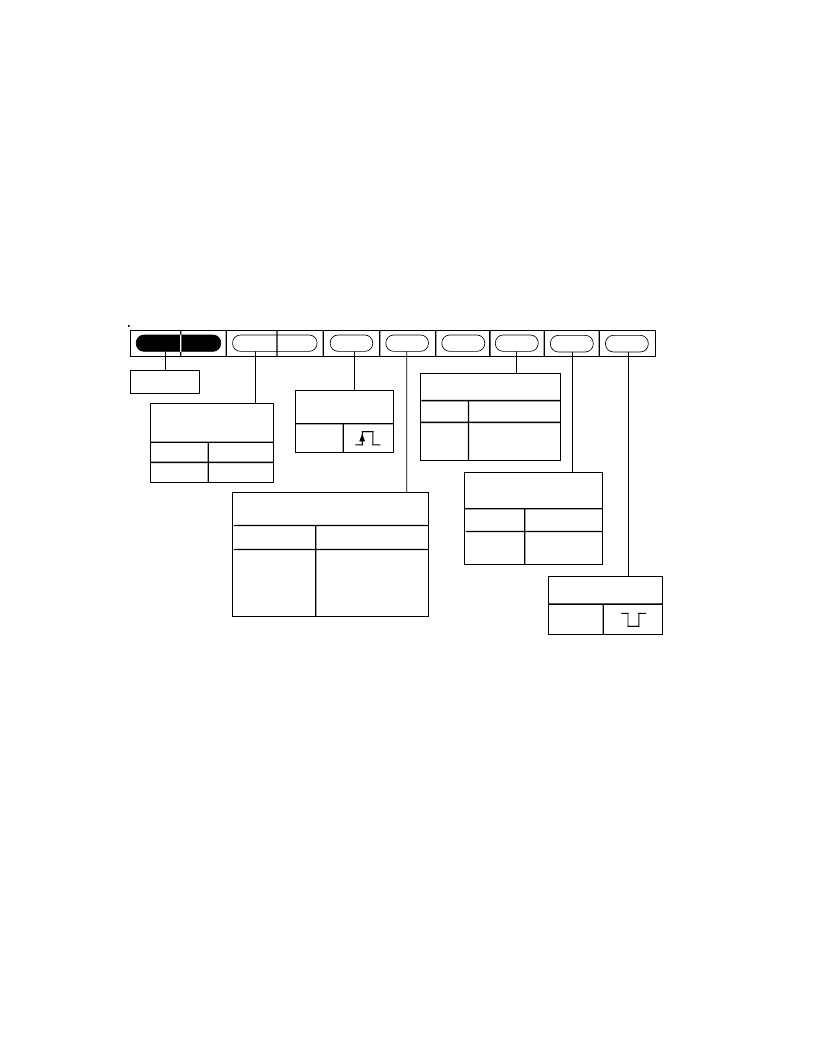
MODE RE GIST E R MR1 (MR19–MR10)
T he mode register is a 10-bit wide register. However for pro-
gramming purposes, it may be considered as an 8-bit wide regis-
ter (MR18 and MR19 are both reserved). It is denoted as
MR17–MR10 for simplification purposes.
T he diagram shows the various operations under the control of
the mode register. T his register can be read from as well written
to. In read mode, if MR18 and MR19 are read back, they are
both returned as zeros.
Mode Register (MR17–MR10) Bit Description
Reset Control (MR10)
T his bit is used to reset the pixel port sampling sequence. T his
ensures that the pixel sequence ABCD starts at A. It is reset by
writing a “1” followed by a “0” followed by a “1.” T his bit must
be run through this cycle during the initialization sequence.
RAM-DAC Resolution Control (MR11)
When this is programmed with a “1,” the RAM is 30 bits deep
(10 bits each for red, green and blue) and each of the three
DACs is configured for 10-bit resolution. When MR11 is
programmed with a “0,” the RAM is 24-bits deep (8 bits each
for red, green and blue) and the DACs are configured for 8-bit
resolution. T he two LSBs of the 10-bit DACs are pulled down
to zero in 8-bit RAM-DAC mode.
MPU Databus Width (MR12)
T his bit determines the width of the MPU port. It is configured
as either a 10-bit wide (D9–D0) or 8-bit wide (D7–D0) bus.
10-bit data can be written to the device when configured in
8-bit wide mode. T he 8 MSBs are first written on D7–D0, then
the two LSBs are written over D1–D0. Bits D9–D8 are zeros in
8-bit mode.
Operational Mode Control (MR14–MR13)
When MR14 is “0” and MR13 is “1,” the part operates in
normal mode.
Calibrate LOADIN (MR15)
T his bit automatically calibrates the onboard L OADIN/
LOADOUT synchronization circuit. A “0” to “1” transition
initiates calibration. T his bit is set to “0” in normal operation.
See “Pipeline Delay and Calibration” section. T his bit must be
run through this cycle during the initialization sequence.
MR17
MR16
* THESE BITS ARE READ-ONLY RESERVED BITS.
A READ CYCLE WILL RETURN ZEROS "00."
RESERVED*
MR16 PS0
MR17 PS1
PALETTE SELECT
MATCH BITS CONTROL
RAM-DAC
RESOLUTION CONTROL
0 8-BIT
1 10-BIT
MR11
MPU DATA BUS WIDTH
0 8-BIT (D7–D0)
1 10-BIT (D9–D0)
MR12
CALIBRATE
LOADIN
MR15
RESET CONTROL
MR10
OPERATIONAL MODE CONTROL
0 0 RESERVED
0 1 NORMAL OPERATION
1 0 RESERVED
1 1 RESERVED
MR14 MR13
MR19
MR18
MR15
MR14
MR13
MR12
MR11
MR10
Mode Register 1 (MR1) (MR19–MR10)
相關(guān)PDF資料 |
PDF描述 |
|---|---|
| ADV7183 | Video Decoder with 9-Bit ADC(帶9位A/D轉(zhuǎn)換器和自適應(yīng)梳狀濾波器視頻譯碼器) |
| ADV7184 | Multiformat SDTV Video Decoder with Fast Switch Overlay Support |
| ADV7184BSTZ | Multiformat SDTV Video Decoder with Fast Switch Overlay Support |
| ADV7188 | Multiformat SDTV Video Decoder with Fast Switch Overlay Support |
| ADV7189B | Multiformat SDTV Video Decoder |
相關(guān)代理商/技術(shù)參數(shù) |
參數(shù)描述 |
|---|---|
| adv7150ls85 | 制造商:Rochester Electronics LLC 功能描述:220MHZ 3X10 BIT VIDEO DAC - Bulk 制造商:Analog Devices 功能描述: |
| ADV7151 | 制造商:AD 制造商全稱:Analog Devices 功能描述:CMOS 220 MHz Pseudo-Color Graphics Triple 10-Bit Video RAM-DAC |
| ADV7151KS110 | 制造商:未知廠家 制造商全稱:未知廠家 功能描述:Video DAC with Color Palette (RAMDAC) |
| ADV7151KS135 | 制造商:未知廠家 制造商全稱:未知廠家 功能描述:Video DAC with Color Palette (RAMDAC) |
| ADV7151KS170 | 制造商:未知廠家 制造商全稱:未知廠家 功能描述:Video DAC with Color Palette (RAMDAC) |
發(fā)布緊急采購,3分鐘左右您將得到回復(fù)。