- 您現(xiàn)在的位置:買賣IC網(wǎng) > PDF目錄374037 > ADSP-21MOD980N (Analog Devices, Inc.) MultiPort Internet Gateway Processor PDF資料下載
參數(shù)資料
| 型號: | ADSP-21MOD980N |
| 廠商: | Analog Devices, Inc. |
| 英文描述: | MultiPort Internet Gateway Processor |
| 中文描述: | 通寶互聯(lián)網(wǎng)網(wǎng)關(guān)處理器 |
| 文件頁數(shù): | 4/42頁 |
| 文件大小: | 566K |
| 代理商: | ADSP-21MOD980N |
第1頁第2頁第3頁當前第4頁第5頁第6頁第7頁第8頁第9頁第10頁第11頁第12頁第13頁第14頁第15頁第16頁第17頁第18頁第19頁第20頁第21頁第22頁第23頁第24頁第25頁第26頁第27頁第28頁第29頁第30頁第31頁第32頁第33頁第34頁第35頁第36頁第37頁第38頁第39頁第40頁第41頁第42頁
4
6/2001
REV. PrB
For current information contact Analog Devices at (800) ANALOGD
ADSP-21mod980N
PRELIMINARY TECHNICAL DATA
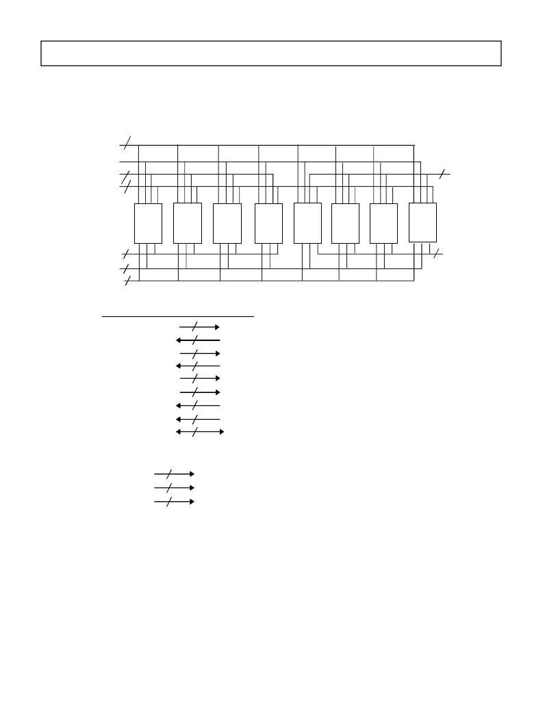
ARCHITECTURE OVERVIEW
Figure 2 on page 4 is a functional block diagram of the
ADSP-21mod980N. It contains eight independent digital
signal processors.
Every modem processor has:
A DSP core
256K bytes of RAM
Two serial ports
An IDMA host.
The signals of each modem processor are accessed through
the external pins of the ADSP-21mod980N. Some signals
are bussed with the signals of the other processors and are
accessed through a single external pin. Other signals remain
separate and they are accessed through separate external
pins for each processor.
The arrangement of the eight modem processors in the
ADSP-21mod980N makes one basic configuration possi-
ble: a
slave
configuration. In this configuration, the data
pins of all eight processors connect to a single bus structure.
Figure 2. ADSP-21mod980N Functional Block Diagram
IAD<15:0>, IDMA CNTL
PF<0:2>/MODE A:C
20
3
2188N
2188N
2188N
2188N
2188N
17
2188N
4
4
8
4
2188N
2188N
20
SPORT1
SPORT0A
CLKIN
EMULATOR
SUBTOTAL = 177 SIGNAL BALLS
SIGNALS ROUTED TO EACH RESPECTIVE DIE
8
BG <8:1>
8
BR <8:1>
EE <8:1>
8
IS <8:1>
8
RESET <8:1>
8
CLKOUT <8:1>
8
TFS0 <8:1>
8
DT1 <8:1>
8
INTERRUPTS <8:1>
32
22
VDDINT
44
VDDEXT
SUBTOTAL = 175 POWER BALLS
TOTAL = 352 BALLS
109
GND
DATA<23:8>, A<0>
IAD <15:0>,
IDMA CNTL
SPORT0B
IDMA CNTL = IAL, IRD, IWR, IACK
INTERRUPTS = IRQE (PF4), IRQL0(PF5), IRQL1(PF6), IRQ2(PF7)
EMULATOR = EMS, EINT, ELIN, EBR, EBG, ECLK
ELOUT, ERESET
SPORT0A, SPORT 0B
= RFS0, DR0, DT0, SCKL0
SPORT1 = RFS1, TFS1, DR1, SCKL1
NOTE:
1. PWD AND PF3/MODE D ARE TIED HIGH
DSP 1
DSP 2
DSP 3
DSP 4
DSP 5
DSP 6
DSP 7
DSP 8
相關(guān)PDF資料 |
PDF描述 |
|---|---|
| ADSP-21MOD980N-000 | CAP 27PF 100V 10% X7R AXIAL BULK M-MIL-PRF-39014 |
| ADSP-21MSP58BST-104 | DSP Microcomputers |
| ADSP-BF531 | Blackfin Embedded Processor |
| ADSP-BF531SBBC400 | Metal Connector Backshell |
| ADSP-BF531SBBZ400 | Blackfin Embedded Processor |
相關(guān)代理商/技術(shù)參數(shù) |
參數(shù)描述 |
|---|---|
| ADSP-21MSP50ABG-52 | 制造商:Analog Devices 功能描述: |
| adsp-21msp50akg-52 | 制造商:Rochester Electronics LLC 功能描述:- Bulk 制造商:Analog Devices 功能描述: |
| ADSP-21MSP50BG-52 | 制造商:Rochester Electronics LLC 功能描述:- Bulk |
| ADSP-21MSP50KG-52 | 制造商:Rochester Electronics LLC 功能描述:- Bulk |
| ADSP-21MSP52-520010 | 制造商:Analog Devices 功能描述: |
發(fā)布緊急采購,3分鐘左右您將得到回復(fù)。