- 您現(xiàn)在的位置:買賣IC網(wǎng) > PDF目錄17098 > ADS8361EVM (Texas Instruments)EVAL MOD FOR ADS8361 PDF資料下載
參數(shù)資料
| 型號: | ADS8361EVM |
| 廠商: | Texas Instruments |
| 文件頁數(shù): | 5/29頁 |
| 文件大小: | 0K |
| 描述: | EVAL MOD FOR ADS8361 |
| 產(chǎn)品培訓(xùn)模塊: | Data Converter Basics |
| 標(biāo)準(zhǔn)包裝: | 1 |
| ADC 的數(shù)量: | 2 |
| 位數(shù): | 16 |
| 采樣率(每秒): | 500k |
| 數(shù)據(jù)接口: | 串行 |
| 輸入范圍: | 0 ~ 5 V |
| 在以下條件下的電源(標(biāo)準(zhǔn)): | 150mW @ 500kSPS |
| 工作溫度: | -40°C ~ 125°C |
| 已用 IC / 零件: | ADS8361 |
| 已供物品: | 板 |
| 產(chǎn)品目錄頁面: | 893 (CN2011-ZH PDF) |
| 相關(guān)產(chǎn)品: | ADS8361IRHBTG4-ND - IC ADC DUAL 16BIT 500KSPS 32VQFN ADS8361IRHBRG4-ND - IC ADC DUAL 16BIT 500KSPS 32VQFN ADS8361IRHBR-ND - IC ADC DUAL 16BIT 500KSPS 32VQFN ADS8361IDBQRG4-ND - IC ADC DUAL 16BIT 500KSPS 24QSOP ADS8361IDBQR-ND - IC ADC DUAL 16BIT 500KSPS 24QSOP ADS8361IDBQG4-ND - IC ADC DUAL 16BIT 500KSPS 24QSOP 296-17411-6-ND - IC ADC DUAL 16BIT 500KSPS 32VQFN 296-17411-1-ND - IC ADC DUAL 16BIT 500KSPS 32VQFN 296-17411-2-ND - IC ADC DUAL 16BIT 500KSPS 32VQFN 296-13812-5-ND - IC ADC DUAL 16BIT 500KSPS 24QSOP |
| 其它名稱: | 296-19922 ADS8361EVM-ND |
第1頁第2頁第3頁第4頁當(dāng)前第5頁第6頁第7頁第8頁第9頁第10頁第11頁第12頁第13頁第14頁第15頁第16頁第17頁第18頁第19頁第20頁第21頁第22頁第23頁第24頁第25頁第26頁第27頁第28頁第29頁
ADS8361
13
SBAS230E
www.ti.com
tion). Twenty clock cycles are required to perform a single
conversion. Immediately following CONVST switching to
HIGH, the ADS8361 will switch from the sample mode to the
hold mode asynchronous to the external clock. The BUSY
output pin will then go HIGH and remain HIGH for the
duration of the conversion cycle. On the falling edge of the
first cycle of the external clock, the ADS8361 will latch in the
address for the next conversion cycle depending on the
status of the A0 pin (HIGH = Channel 1, LOW = Channel 0).
The address must be selected 15ns prior to the falling edge of
cycle one of the external clock and must remain ‘held’ for 15ns
following the clock edge. For maximum throughput time, the
CONVST and RD pins should be tied together. CS must be
brought LOW to enable the CONVST and RD inputs. Data will
be valid on the falling edge of all 20 clock cycles per conver-
sion. The first bit of data will be a status flag for either Channel
0 or 1, the second bit will be a second status flag for either
Channel A or B. First and second bit will be 0 in Mode I. See
Table II below. The subsequent data will be MSB-first through
the LSB, followed by two zeros (see Table III and Figures 9
and 10).
CLOCK CYCLE
1
2
3
4
5
6
7
8
9
10
11
12
13
14
15
16
17
18
19
20
SERIAL DATA CH0 OR CH1 CHA OR CHB DB15 DB14 DB13 DB12 DB11 DB10 DB9 DB8
DB7
DB6
DB5
DB4
DB3
DB2 DB1
DB0
0
TABLE III. Serial Data Output Format.
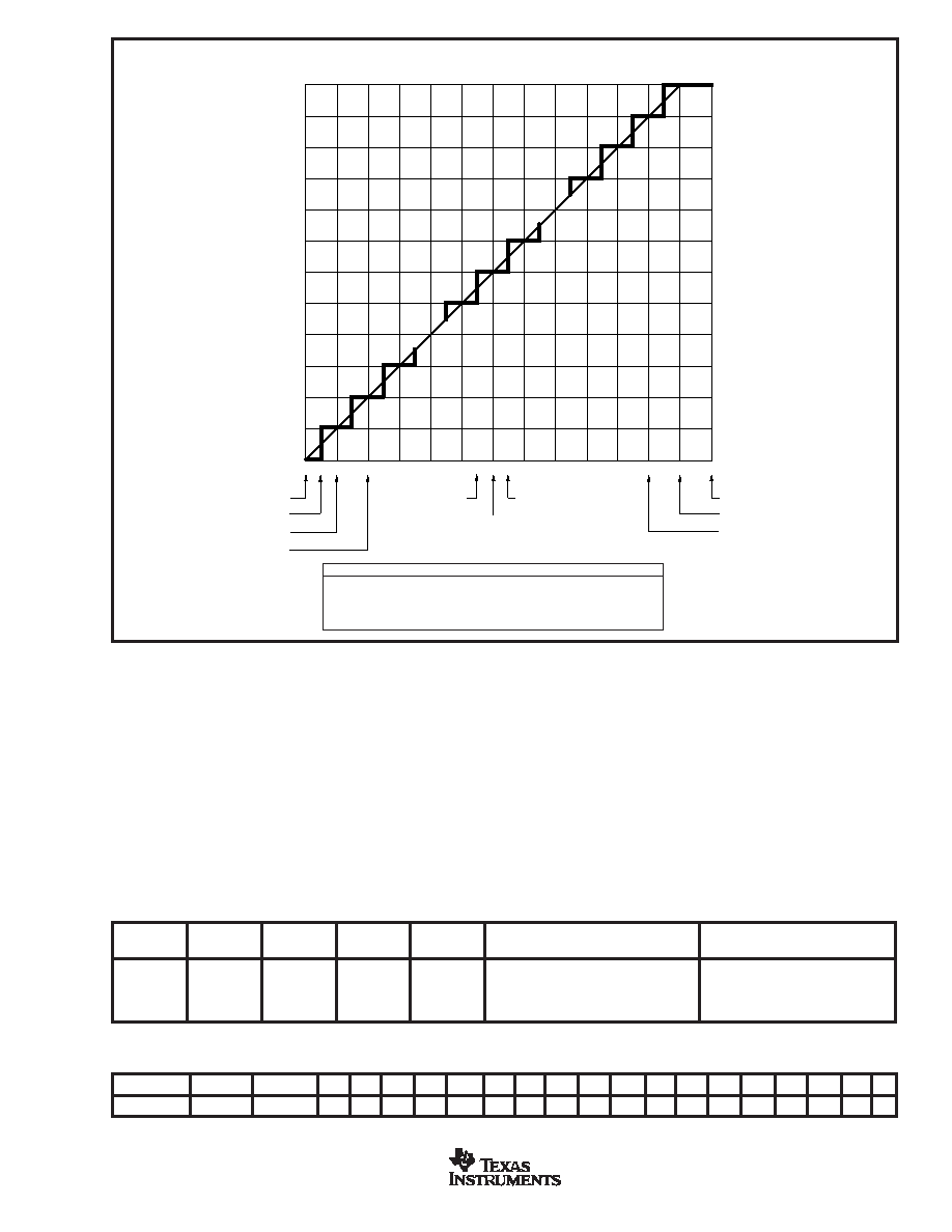
FIGURE 8. Ideal Conversion Characteristics (Condition: Single Ended, VCM = chXX– = 2.5V, VREF = 2.5V)
BIT 1
BIT 2
MODE
M0
M1
CH0/1
CHA/B
CHANNEL SELECTION
DATA OUTPUT
10000
Ch0/1 Selected by A0
On Data A and B
2010
0 = A/1 = B
Ch0/1 Selected by A0
Sequentially on Data A
3
1
0
0/1
0
Ch0/1 Alternating
On Data A and B
4
1
0/1
0 = A/1 = B
Ch0/1 Alternating
Sequentially on Data A
TABLE II. Mode Selection.
0111 1111 1111 1111
0111 1111 1111 1110
0111 1111 1111 1101
0000 0000 0000 0001
0000 0000 0000 0000
1000 0000 0000 0010
1000 0000 0000 0001
1000 0000 0000 0000
1111 1111 1111 1111
Binary Two’s Complement
BTC
Digital
Output
Code
VNFS = VCM – VREF = 0V
0.000038V
0.000076V
0.000152V
2.499962V
2.500038V
VBPZ = 2.5V
Unipolar Analog Input Voltage
1LSB = 76μV
VCM = 2.5V
VREF = 2.5V
4.999848V
VPFS – 1LSB = 4.999924V
VPFS = VCM + VREF = 5V
0
1
2
32767
32768
32769
65533
65534
65535
Step
16-BIT
Bipolar Input, Binary Two’s Complement Output: (BTC)
Negative Full-Scale Code
Bipolar Zero Code
Positive Full-Scale Code
= VNFS = 8000H, Vcode = VCM – VREF
= VBPZ = 0000H, Vcode = VCM
= VPFS = 7FFFH, Vcode = (VCM + VREF)– 1LSB
相關(guān)PDF資料 |
PDF描述 |
|---|---|
| RBM12DCBN | CONN EDGECARD 24POS R/A .156 SLD |
| R-729.0D | CONV DC/DC 2A 12-28VIN 9V |
| SK102M025ST | CAP ALUM 1000UF 25V 20% RADIAL |
| R-726.5P | CONV DC/DC 2A 8.5-28VIN 6.5V |
| DK-S6-EMBD-G | DEV KIT EMBEDDED SPARTAN 6 |
相關(guān)代理商/技術(shù)參數(shù) |
參數(shù)描述 |
|---|---|
| ADS8361IBDBQ | 制造商:Rochester Electronics LLC 功能描述:DUAL 250KHZ-16 BIT, 2+2 CHANNEL - Bulk 制造商:Texas Instruments 功能描述:DUAL 250KHZ-16 BIT, 2+2 CHANNEL - Rail/Tube |
| ADS8361IBDBQR | 制造商:Texas Instruments 功能描述:DUAL 250KHZ-16 BIT, 2+2 CHANNEL - Tape and Reel |
| ADS8361IDBQ | 功能描述:模數(shù)轉(zhuǎn)換器 - ADC 16-Bit 500 kSPS 2 ADC 4ch ser out RoHS:否 制造商:Texas Instruments 通道數(shù)量:2 結(jié)構(gòu):Sigma-Delta 轉(zhuǎn)換速率:125 SPs to 8 KSPs 分辨率:24 bit 輸入類型:Differential 信噪比:107 dB 接口類型:SPI 工作電源電壓:1.7 V to 3.6 V, 2.7 V to 5.25 V 最大工作溫度:+ 85 C 安裝風(fēng)格:SMD/SMT 封裝 / 箱體:VQFN-32 |
| ADS8361IDBQG4 | 功能描述:模數(shù)轉(zhuǎn)換器 - ADC 16-Bit 500 kSPS 2 ADC 4ch ser out RoHS:否 制造商:Texas Instruments 通道數(shù)量:2 結(jié)構(gòu):Sigma-Delta 轉(zhuǎn)換速率:125 SPs to 8 KSPs 分辨率:24 bit 輸入類型:Differential 信噪比:107 dB 接口類型:SPI 工作電源電壓:1.7 V to 3.6 V, 2.7 V to 5.25 V 最大工作溫度:+ 85 C 安裝風(fēng)格:SMD/SMT 封裝 / 箱體:VQFN-32 |
| ADS8361IDBQR | 功能描述:模數(shù)轉(zhuǎn)換器 - ADC 16-Bit 500 kSPS 2 ADC 4ch ser out RoHS:否 制造商:Texas Instruments 通道數(shù)量:2 結(jié)構(gòu):Sigma-Delta 轉(zhuǎn)換速率:125 SPs to 8 KSPs 分辨率:24 bit 輸入類型:Differential 信噪比:107 dB 接口類型:SPI 工作電源電壓:1.7 V to 3.6 V, 2.7 V to 5.25 V 最大工作溫度:+ 85 C 安裝風(fēng)格:SMD/SMT 封裝 / 箱體:VQFN-32 |
發(fā)布緊急采購,3分鐘左右您將得到回復(fù)。