- 您現(xiàn)在的位置:買賣IC網(wǎng) > PDF目錄17098 > ADS8361EVM (Texas Instruments)EVAL MOD FOR ADS8361 PDF資料下載
參數(shù)資料
| 型號: | ADS8361EVM |
| 廠商: | Texas Instruments |
| 文件頁數(shù): | 4/29頁 |
| 文件大小: | 0K |
| 描述: | EVAL MOD FOR ADS8361 |
| 產(chǎn)品培訓(xùn)模塊: | Data Converter Basics |
| 標(biāo)準(zhǔn)包裝: | 1 |
| ADC 的數(shù)量: | 2 |
| 位數(shù): | 16 |
| 采樣率(每秒): | 500k |
| 數(shù)據(jù)接口: | 串行 |
| 輸入范圍: | 0 ~ 5 V |
| 在以下條件下的電源(標(biāo)準(zhǔn)): | 150mW @ 500kSPS |
| 工作溫度: | -40°C ~ 125°C |
| 已用 IC / 零件: | ADS8361 |
| 已供物品: | 板 |
| 產(chǎn)品目錄頁面: | 893 (CN2011-ZH PDF) |
| 相關(guān)產(chǎn)品: | ADS8361IRHBTG4-ND - IC ADC DUAL 16BIT 500KSPS 32VQFN ADS8361IRHBRG4-ND - IC ADC DUAL 16BIT 500KSPS 32VQFN ADS8361IRHBR-ND - IC ADC DUAL 16BIT 500KSPS 32VQFN ADS8361IDBQRG4-ND - IC ADC DUAL 16BIT 500KSPS 24QSOP ADS8361IDBQR-ND - IC ADC DUAL 16BIT 500KSPS 24QSOP ADS8361IDBQG4-ND - IC ADC DUAL 16BIT 500KSPS 24QSOP 296-17411-6-ND - IC ADC DUAL 16BIT 500KSPS 32VQFN 296-17411-1-ND - IC ADC DUAL 16BIT 500KSPS 32VQFN 296-17411-2-ND - IC ADC DUAL 16BIT 500KSPS 32VQFN 296-13812-5-ND - IC ADC DUAL 16BIT 500KSPS 24QSOP |
| 其它名稱: | 296-19922 ADS8361EVM-ND |
第1頁第2頁第3頁當(dāng)前第4頁第5頁第6頁第7頁第8頁第9頁第10頁第11頁第12頁第13頁第14頁第15頁第16頁第17頁第18頁第19頁第20頁第21頁第22頁第23頁第24頁第25頁第26頁第27頁第28頁第29頁
ADS8361
12
SBAS230E
www.ti.com
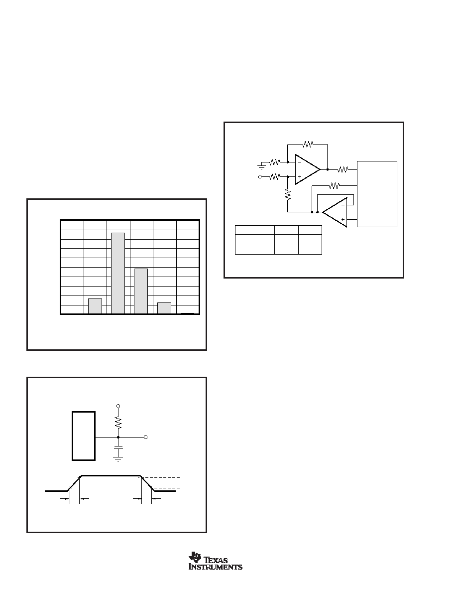
FIGURE 5. Histogram of 8000 Conversions of a DC Input.
FIGURE 6. Test Circuits for Timing Specifications.
FIGURE 7. Level Shift Circuit for Bipolar Input Ranges.
TRANSITION NOISE
The transition noise of the ADS8361 itself is low,
as shown in Figure 5. These histograms were generated by
applying a low-noise DC input and initiating 8000 conversions.
The digital output of the A/D converter will vary in output code
due to the internal noise of the ADS8361. This is true for all 16-
bit, Successive Approximation Register (SAR-type) A/D con-
verters. Using a histogram to plot the output codes, the
distribution should appear bell-shaped with the peak of the bell
curve representing the nominal code for the input value. The
±1σ, ±2σ, and ±3σ distributions will represent the 68.3%,
95.5%, and 99.7%, respectively, of all codes. The transition
noise can be calculated by dividing the number of codes
measured by 6 and this will yield the ±3σ distribution, or
99.7%, of all codes. Statistically, up to three codes could fall
outside the distribution when executing 1000 conversions.
Remember, to achieve this low-noise performance, the peak-
to-peak noise of the input signal and reference must be
< 50μV.
R1
R2
+IN
–IN
REFOUT (pin 11)
2.5V
4kΩ
20kΩ
Bipolar Input
BIPOLAR INPUT
R1
R2
±10V
1kΩ
5kΩ
±5V
2kΩ
10kΩ
±2.5V
4kΩ
20kΩ
OPA227
ADS8361
OPA227
600Ω
DATA
1.4V
Test Point
3kΩ
100pF
CLOAD
tR
DATA
Voltage Waveforms for DATA Rise-and-Fall Times tR, and tF.
VOH
VOL
tF
BIPOLAR INPUTS
The differential inputs of the ADS8361 were designed to
accept bipolar inputs (–VREF and +VREF) around the internal
reference voltage (2.5V), which corresponds to a 0V to 5V
input range with a 2.5V reference. By using a simple op amp
circuit featuring a single amplifier and four external resistors,
the ADS8361 can be configured to except bipolar inputs. The
conventional ±2.5V, ±5V, and ±10V input ranges can be
interfaced to the ADS8361 using the resistor values shown in
Figure 7.
Code (decimal)
5000
4500
4000
3500
3000
2500
2000
1500
1000
500
0
Number
of
Conversions
32761
32762
32764
32763
32765
32766
TIMING AND CONTROL
The operation of the ADS8361 can be configured in four
different modes by using the address pins M0 (pin 14), M1
(pin 15), and A0 (pin 16).
The M0 pin selects between two- and four-channel operation
(in two-channel operation, the A0 pin selects between Chan-
nels 0 and 1; in four-channel operation the A0 pin is ignored
and the channels are switched automatically after each
conversion). The M1 pin selects between having serial data
transmitted simultaneously on both the Serial A data output
(pin 23) and the Serial B data output (pin 22) or having both
channels output data through the Serial A port. The A0 pin
selects either Channel 0 or Channel 1 (see Pin Descriptions
and Serial Output Truth Table for more information).
The next four sections will explain the four different modes of
operation.
Mode I (M0 = 0, M1 = 0)
With the M0 and M1 pins both set to ‘0’, the ADS8361 will
operate in two-channel operation (the A0 pin must be used
to switch between Channels A and B). A conversion is
initiated by bringing CONVST HIGH for a minimum of 15ns.
It is very important that CONVST be brought HIGH a mini-
mum of 10ns prior to a falling edge of the external clock or
5ns after the falling edge. If CONVST is brought HIGH within
this window, it is then uncertain as to when the ADS8361 will
initiate conversion (see Figure 9 for a more detailed descrip-
相關(guān)PDF資料 |
PDF描述 |
|---|---|
| RBM12DCBN | CONN EDGECARD 24POS R/A .156 SLD |
| R-729.0D | CONV DC/DC 2A 12-28VIN 9V |
| SK102M025ST | CAP ALUM 1000UF 25V 20% RADIAL |
| R-726.5P | CONV DC/DC 2A 8.5-28VIN 6.5V |
| DK-S6-EMBD-G | DEV KIT EMBEDDED SPARTAN 6 |
相關(guān)代理商/技術(shù)參數(shù) |
參數(shù)描述 |
|---|---|
| ADS8361IBDBQ | 制造商:Rochester Electronics LLC 功能描述:DUAL 250KHZ-16 BIT, 2+2 CHANNEL - Bulk 制造商:Texas Instruments 功能描述:DUAL 250KHZ-16 BIT, 2+2 CHANNEL - Rail/Tube |
| ADS8361IBDBQR | 制造商:Texas Instruments 功能描述:DUAL 250KHZ-16 BIT, 2+2 CHANNEL - Tape and Reel |
| ADS8361IDBQ | 功能描述:模數(shù)轉(zhuǎn)換器 - ADC 16-Bit 500 kSPS 2 ADC 4ch ser out RoHS:否 制造商:Texas Instruments 通道數(shù)量:2 結(jié)構(gòu):Sigma-Delta 轉(zhuǎn)換速率:125 SPs to 8 KSPs 分辨率:24 bit 輸入類型:Differential 信噪比:107 dB 接口類型:SPI 工作電源電壓:1.7 V to 3.6 V, 2.7 V to 5.25 V 最大工作溫度:+ 85 C 安裝風(fēng)格:SMD/SMT 封裝 / 箱體:VQFN-32 |
| ADS8361IDBQG4 | 功能描述:模數(shù)轉(zhuǎn)換器 - ADC 16-Bit 500 kSPS 2 ADC 4ch ser out RoHS:否 制造商:Texas Instruments 通道數(shù)量:2 結(jié)構(gòu):Sigma-Delta 轉(zhuǎn)換速率:125 SPs to 8 KSPs 分辨率:24 bit 輸入類型:Differential 信噪比:107 dB 接口類型:SPI 工作電源電壓:1.7 V to 3.6 V, 2.7 V to 5.25 V 最大工作溫度:+ 85 C 安裝風(fēng)格:SMD/SMT 封裝 / 箱體:VQFN-32 |
| ADS8361IDBQR | 功能描述:模數(shù)轉(zhuǎn)換器 - ADC 16-Bit 500 kSPS 2 ADC 4ch ser out RoHS:否 制造商:Texas Instruments 通道數(shù)量:2 結(jié)構(gòu):Sigma-Delta 轉(zhuǎn)換速率:125 SPs to 8 KSPs 分辨率:24 bit 輸入類型:Differential 信噪比:107 dB 接口類型:SPI 工作電源電壓:1.7 V to 3.6 V, 2.7 V to 5.25 V 最大工作溫度:+ 85 C 安裝風(fēng)格:SMD/SMT 封裝 / 箱體:VQFN-32 |
發(fā)布緊急采購,3分鐘左右您將得到回復(fù)。