- 您現(xiàn)在的位置:買賣IC網(wǎng) > PDF目錄373980 > ADE7754 (Analog Devices, Inc.) ADE7754 PDF資料下載
參數(shù)資料
| 型號: | ADE7754 |
| 廠商: | Analog Devices, Inc. |
| 英文描述: | ADE7754 |
| 中文描述: | ADE7754 |
| 文件頁數(shù): | 20/44頁 |
| 文件大小: | 630K |
| 代理商: | ADE7754 |
第1頁第2頁第3頁第4頁第5頁第6頁第7頁第8頁第9頁第10頁第11頁第12頁第13頁第14頁第15頁第16頁第17頁第18頁第19頁當前第20頁第21頁第22頁第23頁第24頁第25頁第26頁第27頁第28頁第29頁第30頁第31頁第32頁第33頁第34頁第35頁第36頁第37頁第38頁第39頁第40頁第41頁第42頁第43頁第44頁
REV. PrG 01/03
PRELIMINARY TECHNICAL DATA
ADE7754
–
20
–
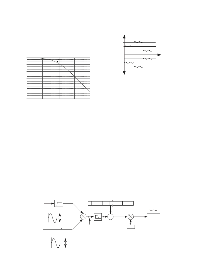
Since LPF2 does not have an ideal “brick wall” frequency
response—see Figure 21, the Active Power signal will have
some ripple due to the instantaneous power signal. This
ripple is sinusoidal and has a frequency equal to twice the line
frequency. Since the ripple is sinusoidal in nature, it is
removed when the Active Power signal is integrated to
calculate the Energy – see
Energy Calculation
.
Frequency
1.0Hz
3.0Hz
10Hz
30Hz
-24
-20
-16
-12
-8
-4
0
d
8Hz
Figure 21
–
Frequency response of the LPF used to filter
Instantaneous Power in each phase
Figure 22 shows the signal processing in each phase for the
Active Power in the ADE7754.
Figure 23 shows the maximum code (Hexadecimal) output
range of the Active Power signal (after AWG). Note that the
output range changes depending on the contents of the Active
Power Gain and Watt Gain registers – see
Current channel
ADC
. The minimum output range is given when the Active
Power Gain and Watt Gain registers contents are equal to
800h and the maximum range is given by writing 7FFh to the
Active Power Gain and Watt Gain registers. These can be
used to calibrate the Active Power (or Energy) calculation in
the ADE7754 for each phase and also the Total Active
Energy -see
Total Active Power calculation
.
0000000h
972474h
D1B717h
68DB8Ch
+ 100% F5
+ 50% FS
AAPGAIN[11:0] or
AWGAIN[11:0]
- 100% FS
- 150% FS
2E48E9h
EC56D5Ch
+ 150% FS
- 50% FS
13A92A4h
000h
7FFh
800h
Active Power
Current channel ± 0.5V / GAIN1
Voltage channel ± 0.5V / GAIN2
Figure 23 – Active Power Calculation Output Range
Power Offset Calibration
The ADE7754 also incorporates an Active Offset register on
each phase (AAPOS, BAPOS and CAPOS). These are
signed 2’s complement 12-bit registers which can be used to
remove offsets in the active power calculations. An offset may
exist in the power calculation due to cross talk between
channels on the PCB or in the IC itself. The offset calibration
allows the contents of the Active Power register to be
maintained at zero when no power is being consumed.
1 LSBs in the Active Power Offset register is equivalent to 1
LSB in the 28-bit Energy bus displayed on Figure 22. Each
time power is added to the internal Active Energy register, the
content of the Active Power Offset register is added -
see Total
Active Power calculation
. Assuming the average value from
LPF2 is 8637BCh (8,796,092d) with full AC scale inputs on
current channel and voltage channel, then 1 LSB in the LPF2
output is equivalent to 0.011% of measurement error at -
60dB down of full scale -
see Calibration of a 3-phase meter
based on the ADE7754
.
1
-100% to + 100% FS
28F5h
HPF
24
LPF2
-100% to +100% FS
28F5C2h
Current Signal - i(t)
Voltage Signal - v(t)
Instantaneous Power Signal - p(t)
MULTIPLIER
Active Power
Signal - P
I
V
D70Bh
D70A3Eh
00h
00h
S
+
24232221
APOS[11:0]
sgn
20
AWG
12
28
D1B717h
sgn sgn sgn sgn210
1V / GAIN1
1V / GAIN2
Figure 22
–
Active Power Signal Processing
相關PDF資料 |
PDF描述 |
|---|---|
| ADE7754AR | ADE7754 |
| ADE7754ARRL | ADE7754 |
| ADE7755AN-REF | Energy Metering IC with Pulse Output |
| ADE7755ARSRL | Energy Metering IC with Pulse Output |
| ADE7755 | Energy Metering IC with Pulse Output |
相關代理商/技術參數(shù) |
參數(shù)描述 |
|---|---|
| ADE7754AR | 制造商:Analog Devices 功能描述:Energy Measurement 24-Pin SOIC W 制造商:Rochester Electronics LLC 功能描述:THREE PHASE ENERGY METER IC W/WATT & VA - Bulk 制造商:Analog Devices 功能描述:IC ENERGY METER |
| ADE7754ARRL | 制造商:Analog Devices 功能描述:Energy Measurement 24-Pin SOIC W T/R 制造商:Rochester Electronics LLC 功能描述:THREE PHASE ENERGY METER IC W/WATT & VA - Bulk |
| ADE7754ARZ | 功能描述:IC ENERGY METERING 3PHASE 24SOIC RoHS:是 類別:集成電路 (IC) >> PMIC - 能量測量 系列:- 產(chǎn)品培訓模塊:Lead (SnPb) Finish for COTS Obsolescence Mitigation Program 標準包裝:2,500 系列:* |
| ADE7754ARZRL | 功能描述:IC ENERGY METERING 3PHASE 24SOIC RoHS:是 類別:集成電路 (IC) >> PMIC - 能量測量 系列:- 產(chǎn)品培訓模塊:Lead (SnPb) Finish for COTS Obsolescence Mitigation Program 標準包裝:2,500 系列:* |
| ADE7755 | 制造商:AD 制造商全稱:Analog Devices 功能描述:Energy Metering IC with Pulse Output |
發(fā)布緊急采購,3分鐘左右您將得到回復。