- 您現(xiàn)在的位置:買賣IC網(wǎng) > PDF目錄373980 > ADE7753 (Analog Devices, Inc.) Active and Apparent Energy Metering IC with di/dt sensor interface PDF資料下載
參數(shù)資料
| 型號: | ADE7753 |
| 廠商: | Analog Devices, Inc. |
| 英文描述: | Active and Apparent Energy Metering IC with di/dt sensor interface |
| 中文描述: | 主動與迪視電能計量IC / dt的傳感器接口 |
| 文件頁數(shù): | 9/38頁 |
| 文件大小: | 449K |
| 代理商: | ADE7753 |
第1頁第2頁第3頁第4頁第5頁第6頁第7頁第8頁當(dāng)前第9頁第10頁第11頁第12頁第13頁第14頁第15頁第16頁第17頁第18頁第19頁第20頁第21頁第22頁第23頁第24頁第25頁第26頁第27頁第28頁第29頁第30頁第31頁第32頁第33頁第34頁第35頁第36頁第37頁第38頁
ADE7753
–9–
REV. PrF 10/02
PRELIMINARY TECHNICAL DATA
ANALOG INPUT S
T he ADE7753 has two fully differential voltage input chan-
nels. T he maximum differential input voltage for input pairs
V1P/V1N and V2P/V2N are ±0.5V. In addition, the maxi-
mum signal level on analog inputs for V1P/V1N and V2P/
V2N are ±0.5V with respect to AGND.
Each analog input channel has a PGA (Programmable Gain
Amplifier) with possible gain selections of 1, 2, 4, 8 and 16.
T he gain selections are made by writing to the Gain regis-
ter—see Figure 2. Bits 0 to 2 select the gain for the PGA in
Channel 1 and the gain selection for the PGA in Channel 2
is made via bits 5 to 7. Figure 1 shows how a gain selection
for Channel 1 is made using the Gain register.
V1P
V1N
Vin
k.Vin
+
-
Σ
+
GAIN[7:0]
Gain (k)
selection
Offset
Adjust
(±50mV)
CH1OS[7:0]
Bit 0 to 5: Sign magnitude coded offset correction
Bit 6: Not used
Bit 7: Digital Integrator (On=1, Off=0; default ON)
Figure 1— PGA in Channel 1
In addition to the PGA, Channel 1 also has a full scale input
range selection for the ADC. T he ADC analog input range
selection is also made using the Gain register—see Figure 2.
As mentioned previously the maximum differential input
voltage is 1V. However, by using bits 3 and 4 in the Gain
register, the maximum ADC input voltage can be set to 0.5V,
0.25V or 0.125V. T his is achieved by adjusting the ADC
reference—see
ADE7753 Reference Circuit
. T able I below sum-
marizes the maximum differential input signal level on
Channel 1 for the various ADC range and gain selections.
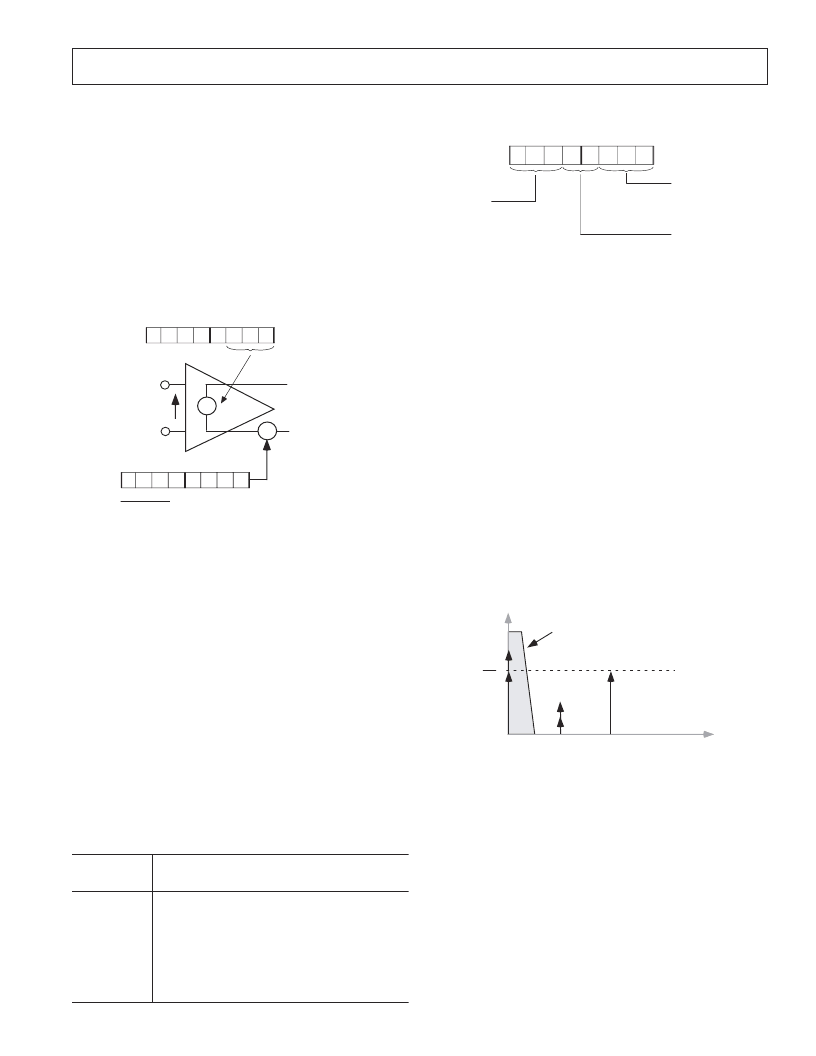
GAIN REGISTER*
Channel 1 and Channel 2 PGA Control
4
5
6
7
ADDR: 0FH
0
1
2
3
PGA 2 Gain Select
000 = x1
001 = x2
010 = x4
011 = x8
100 = x16
0
0
0
0
0
0
0
0
*Register contents show power on defaults
PGA 1 Gain Select
000 = x1
001 = x2
010 = x4
011 = x8
100 = x16
Channel 1 Full Scale Select
00 = 0.5V
01 = 0.25V
10 = 0.125V
Figure 2— ADE7753 Analog Gain register
It is also possible to adjust offset errors on Channel 1 and
C hannel 2 by writing to the Offset C orrection Registers
(C H1OS and C H2OS respectively). T hese registers allow
channel offsets in the range ±20mV to ±50mV (depending on
the gain setting) to be removed. Note that it is not necessary
to perform an offset correction in an Energy measurement
application if HPF in Channel 1 is switched on. Figure 3
shows the effect of offsets on the real power calculation. As
can be seen from Figure 3, an offset on C hannel 1 and
Channel 2 will contribute a dc component after multiplica-
tion. Since this dc component is extracted by L PF 2 to
generate the Active (Real) Power information, the offsets will
have contributed an error to the Active Power calculation.
T his problem is easily avoided by enabling HPF in Channel
1. By removing the offset from at least one channel, no error
component is generated at dc by the multiplication. Error
terms at Cos(w.t) are removed by LPF2 and by integration of
the Active Power signal in the Active Energy register (AEN-
ERGY[23:0]) – see
Energy Calculation
.
V.I
2
frequency (rad/s)
ω
2
ω
0
VOS.IOS
VOS.I
IOS.V
DC component (including error term) is
extracted by the LPF for real power
calculation
Figure 3— Effect of channel offsets on the real power cal-
culation
T he contents of the Offset Correction registers are 6-Bit, sign
and magnitude coded. T he weighting of the L SB size
depends on the gain setting, i.e., 1, 2, 4, 8 or 16. T able II
below shows the correctable offset span for each of the gain
settings and the LSB weight (mV) for the Offset Correction
registers. T he maximum value which can be written to the
offset correction registers is ±31 decimal —see Figure 4.
Figure 4 shows the relationship between the Offset Correc-
tion register contents and the offset (mV) on the analog inputs
for a gain setting of one. In order to perform an offset
adjustment, T he analog inputs should be first connected to
AGND, and there should be no signal on either Channel 1
or Channel 2. A read from Channel 1 or Channel 2 using the
Max Signal
C hannel 1
ADC Input Range Selection
0. 5V
0. 25V
0. 125V
0.5V
0.25V
0.125V
0.0625V
0.0313V
0.0156V
0.00781V
Gain = 1
Gain = 2
Gain = 4
Gain = 8
Gain = 16 Gain = 8
—
—
—
Gain = 1
Gain = 2
Gain = 4
—
—
Gain = 1
Gain = 2
Gain = 4
Gain = 16 Gain = 8
—
Gain = 16
T able I
Maximum input signal levels for C hannel 1
相關(guān)PDF資料 |
PDF描述 |
|---|---|
| ADE7753ARS | Active and Apparent Energy Metering IC with di/dt sensor interface |
| ADE7753ARSRL | Active and Apparent Energy Metering IC with di/dt sensor interface |
| ADE7754 | ADE7754 |
| ADE7754AR | ADE7754 |
| ADE7754ARRL | ADE7754 |
相關(guān)代理商/技術(shù)參數(shù) |
參數(shù)描述 |
|---|---|
| ADE7753_10 | 制造商:AD 制造商全稱:Analog Devices 功能描述:Single-Phase Multifunction Metering IC with di/dt Sensor Interface |
| ADE7753ARS | 制造商:Analog Devices 功能描述:Single Phase Multifunction Metering IC 20-Pin SSOP 制造商:Rochester Electronics LLC 功能描述:- Bulk 制造商:Analog Devices 功能描述:IC SEMICONDUTOR ((NS)) |
| ADE7753ARSRL | 制造商:Analog Devices 功能描述:Single Phase Multifunction Metering IC 20-Pin SSOP T/R 制造商:Rochester Electronics LLC 功能描述:- Bulk |
| ADE7753ARSZ | 功能描述:IC ENERGY METERING 1PHASE 20SSOP RoHS:是 類別:集成電路 (IC) >> PMIC - 能量測量 系列:- 產(chǎn)品培訓(xùn)模塊:Lead (SnPb) Finish for COTS Obsolescence Mitigation Program 標(biāo)準(zhǔn)包裝:2,500 系列:* |
| ADE7753ARSZ | 制造商:Analog Devices 功能描述:ENERGY METERING IC |
發(fā)布緊急采購,3分鐘左右您將得到回復(fù)。