- 您現(xiàn)在的位置:買賣IC網(wǎng) > PDF目錄373980 > ADE7753 (Analog Devices, Inc.) Active and Apparent Energy Metering IC with di/dt sensor interface PDF資料下載
參數(shù)資料
| 型號(hào): | ADE7753 |
| 廠商: | Analog Devices, Inc. |
| 英文描述: | Active and Apparent Energy Metering IC with di/dt sensor interface |
| 中文描述: | 主動(dòng)與迪視電能計(jì)量IC / dt的傳感器接口 |
| 文件頁(yè)數(shù): | 18/38頁(yè) |
| 文件大小: | 449K |
| 代理商: | ADE7753 |
第1頁(yè)第2頁(yè)第3頁(yè)第4頁(yè)第5頁(yè)第6頁(yè)第7頁(yè)第8頁(yè)第9頁(yè)第10頁(yè)第11頁(yè)第12頁(yè)第13頁(yè)第14頁(yè)第15頁(yè)第16頁(yè)第17頁(yè)當(dāng)前第18頁(yè)第19頁(yè)第20頁(yè)第21頁(yè)第22頁(yè)第23頁(yè)第24頁(yè)第25頁(yè)第26頁(yè)第27頁(yè)第28頁(yè)第29頁(yè)第30頁(yè)第31頁(yè)第32頁(yè)第33頁(yè)第34頁(yè)第35頁(yè)第36頁(yè)第37頁(yè)第38頁(yè)
ADE7753
–18–
REV. PrF 10/02
PRELIMINARY TECHNICAL DATA
However, despite being internally phase compensated the
AD E7753 must work with transducers which may have
inherent phase errors. For example a phase error of 0.1° to
0.3° is not uncommon for a CT (Current T ransformer).
T hese phase errors can vary from part to part and they must
be corrected in order to perform accurate power calculations.
T he errors associated with phase mismatch are particularly
noticeable at low power factors. T he ADE7753 provides a
means of digitally calibrating these small phase errors. T he
ADE7753 allows a small time delay or time advance to be
introduced into the signal processing chain in order to
compensate for small phase errors. Because the compensa-
tion is in time, this technique should only be used for small
phase errors in the range of 0.1° to 0.5°. Correcting large
phase errors using a time shift technique can introduce
significant phase errors at higher harmonics.
T he Phase C alibration register (PH C AL [5:0]) is a 2’s
complement signed single byte register which has values
ranging from 21h (-31 in Decimal) to 1Fh (31 in Decimal).
T he register is centered at 0Dh, so that writing 0Dh to the
register gives zero delay. By changing the PHCAL register,
the time delay in the Channel 2 signal path can change from
–100.8μs to +33.6μs (CLK IN = 3.579545MHz). One LSB
is equivalent to 2.22μs time delay or advance. With a line
frequency of 60Hz this gives a phase resolution of 0.048° at
the fundamental (i.e., 360°
×
2.22μs
×
60Hz). Figure 27
illustrates how the phase compensation is used to remove a
0.1° phase lead in Channel 1 due to the external transducer.
In order to cancel the lead (0.1°) in Channel 1, a phase lead
must also be introduced into Channel 2. T he resolution of the
phase adjustment allows the introduction of a phase lead in
increment of 0.048°. T he phase lead is achieved by introduc-
ing a time advance into Channel 2. A time advance of 4.48μs
is made by writing -2 (0Bh) to the time delay block, thus
reducing the amount of time delay by 4.48μs, or equivalently,
a phase lead of approximately 0.1° at line frequency of 60Hz.
0Bh represents -2 because the register is centered with zero
at 0Dh.
0
0
0
1
1
0
1
5
V2P
V2N
ADC 2
PGA2
1
V2
24
LPF2
HPF
V1P
V1N
ADC 1
PGA1
V1
24
PHs to +34
-100
μ
s
Delay Block
4.48
μ
s / LSB
V1
V2
60Hz
Channel 2 delay
reduced by 4.48
μ
s
(0.1
8
lead at 60Hz)
0Bh in PHCAL[5:0]
V2
V1
0.1
8
60Hz
Figure 27 – Phase Calibration
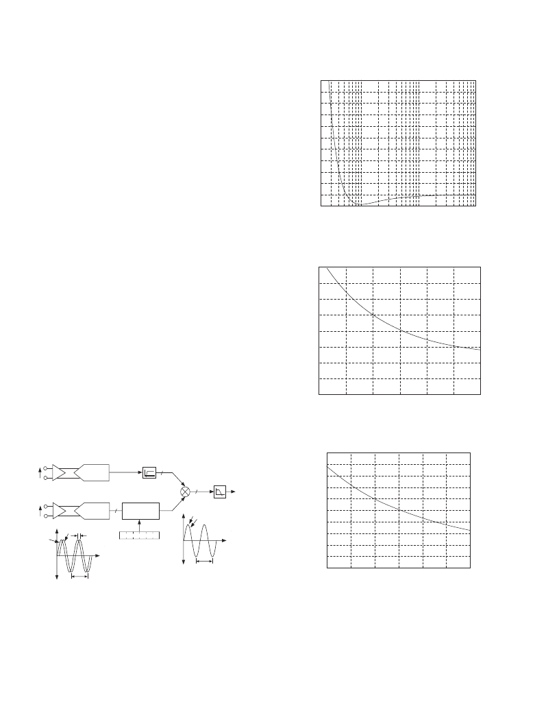
10
2
10
3
10
4
-0.1
0
0.1
0.2
0.3
0.4
0.5
0.6
0.7
0.8
0.9
FREQUENCY-Hz
P
Figure 28 – Combined Phase Response of the HPF & Phase
Compensation (10Hz to 1kHz)
40
45
50
55
60
65
70
-0.2
-0.15
-0.1
-0.05
0.05
0.1
0.15
0.2
FREQUENCY-Hz
P
Figure 29 – Combined Phase Response of the HPF & Phase
Compensation (40Hz to 70Hz)
40
45
50
55
60
65
70
0
0.02
0.04
0.06
0.08
0.1
0.12
0.14
0.16
0.18
0.2
FREQUENCY-Hz
G
Figure 30 – Combined Gain Response of the
HPF & Phase Compensation
A C T IV E P OW E R C A L C UL A T ION
Power is defined as the rate of energy flow from source to
load. It is defined as the product of the voltage and current
waveforms. T he resulting waveform is called the instanta-
neous power signal and it is equal to the rate of energy flow
at every instant of time. T he unit of power is the watt or joules/
相關(guān)PDF資料 |
PDF描述 |
|---|---|
| ADE7753ARS | Active and Apparent Energy Metering IC with di/dt sensor interface |
| ADE7753ARSRL | Active and Apparent Energy Metering IC with di/dt sensor interface |
| ADE7754 | ADE7754 |
| ADE7754AR | ADE7754 |
| ADE7754ARRL | ADE7754 |
相關(guān)代理商/技術(shù)參數(shù) |
參數(shù)描述 |
|---|---|
| ADE7753_10 | 制造商:AD 制造商全稱:Analog Devices 功能描述:Single-Phase Multifunction Metering IC with di/dt Sensor Interface |
| ADE7753ARS | 制造商:Analog Devices 功能描述:Single Phase Multifunction Metering IC 20-Pin SSOP 制造商:Rochester Electronics LLC 功能描述:- Bulk 制造商:Analog Devices 功能描述:IC SEMICONDUTOR ((NS)) |
| ADE7753ARSRL | 制造商:Analog Devices 功能描述:Single Phase Multifunction Metering IC 20-Pin SSOP T/R 制造商:Rochester Electronics LLC 功能描述:- Bulk |
| ADE7753ARSZ | 功能描述:IC ENERGY METERING 1PHASE 20SSOP RoHS:是 類別:集成電路 (IC) >> PMIC - 能量測(cè)量 系列:- 產(chǎn)品培訓(xùn)模塊:Lead (SnPb) Finish for COTS Obsolescence Mitigation Program 標(biāo)準(zhǔn)包裝:2,500 系列:* |
| ADE7753ARSZ | 制造商:Analog Devices 功能描述:ENERGY METERING IC |
發(fā)布緊急采購(gòu),3分鐘左右您將得到回復(fù)。