- 您現(xiàn)在的位置:買賣IC網(wǎng) > PDF目錄375248 > AD9772AST (ANALOG DEVICES INC) 14-Bit, 150 MSPS TxDAC⑩ with 2x Interpolation Filter PDF資料下載
參數(shù)資料
| 型號: | AD9772AST |
| 廠商: | ANALOG DEVICES INC |
| 元件分類: | DAC |
| 英文描述: | 14-Bit, 150 MSPS TxDAC⑩ with 2x Interpolation Filter |
| 中文描述: | PARALLEL, WORD INPUT LOADING, 0.011 us SETTLING TIME, 14-BIT DAC, PQFP48 |
| 封裝: | PLASTIC, LQFP-48 |
| 文件頁數(shù): | 18/30頁 |
| 文件大小: | 340K |
| 代理商: | AD9772AST |
第1頁第2頁第3頁第4頁第5頁第6頁第7頁第8頁第9頁第10頁第11頁第12頁第13頁第14頁第15頁第16頁第17頁當(dāng)前第18頁第19頁第20頁第21頁第22頁第23頁第24頁第25頁第26頁第27頁第28頁第29頁第30頁
REV. 0
AD9772
–18–
complementary output with the full-scale current split between
the two outputs as a function of the input code.
The digital interface is implemented using an edge-triggered
master slave latch and is designed to support an input data rate
as high as 150 MSPS. The clock can be operated at any duty
cycle that meets the specified latch pulsewidth as shown in Figures
1a and 1b. The setup and hold times can also be varied within
the clock cycle as long as the specified minimum times are
met. The digital inputs (excluding CLK+ and CLK–) are CMOS-
compatible with its logic thresholds, V
THRESHOLD,
set to approxi-
mately half the digital positive supply (i.e., DVDD or CLKVDD)
or
V
THRESHOLD
= DVDD
/2 (
±
20%)
The internal digital circuitry of the AD9772 is capable of operating
over a digital supply range of 2.7 V to 3.6 V. As a result, the
digital inputs can also accommodate TTL levels when DVDD is
set to accommodate the maximum high level voltage of the TTL
drivers V
OH(MAX)
. Although a DVDD of 3.3 V will typically
ensure proper compatibility with most TTL logic families, a
series 200
resistors are recommended between the TTL logic
driver and digital inputs to limit the peak current through the
ESD protection diodes if V
OH(MAX)
exceeds DVDD by more
than 300 mV. Figure 36 shows the equivalent digital input cir-
cuit for the data and control inputs.
DIGITAL
INPUT
DVDD
Figure 36. Equivalent Digital Input
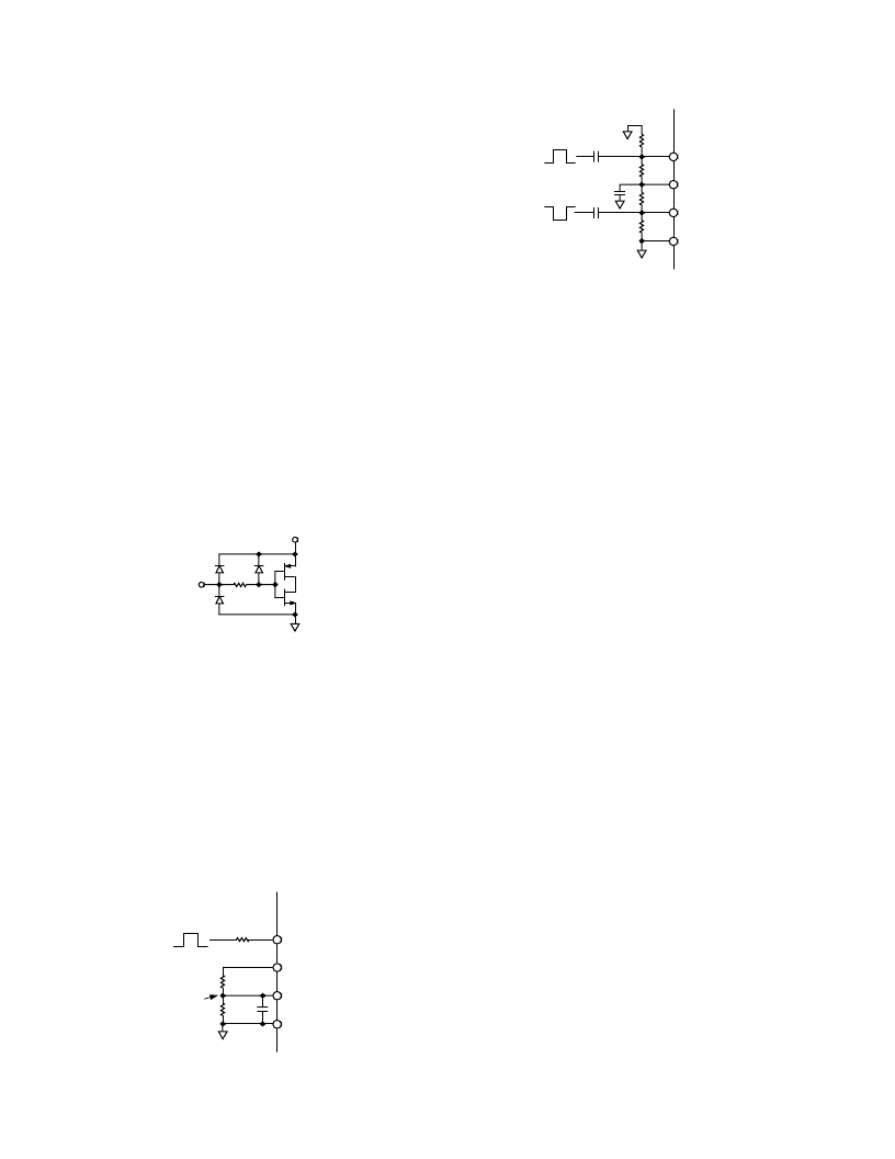
The AD9772 features a flexible differential clock input operat-
ing from separate supplies (i.e., CLKVDD, CLKCOM) to
achieve optimum jitter performance. The two clock inputs,
CLK+ and CLK–, can be driven from a single-ended or
differential clock source. For single-ended operation, CLK+
should be driven by a single-ended logic source while CLK–
should be set to the logic source’s threshold voltage via a resistor
divider/capacitor network referenced to CLKVDD as shown in
Figure 37. For differential operation, both CLK+ and CLK–
should be biased to CLKVDD/2 via a resistor divider network
as shown in Figure 38. An RF transformer as shown in Figure 3
can also be used to convert a single-ended clock input to a dif-
ferential clock input.
R
SERIES
V
THRESHHOLD
AD9772
CLK+
CLKVDD
CLK–
CLKCOM
0.1
m
F
1k
V
1k
V
Figure 37. Single-Ended Clock Interface
AD9772
CLK+
CLKVDD
CLK–
CLKCOM
0.1
m
F
0.1
m
F
0.1
m
F
1k
V
1k
V
1k
V
1k
V
ECL/PECL
Figure 38. Differential Clock Interface
The quality of the clock and data input signals are important in
achieving the optimum performance. The external clock driver
circuitry should provide the AD9772 with a low jitter clock
input meeting the min/max logic levels while providing fast
edges. Although fast clock edges help minimize any jitter that
will manifest itself as phase noise on a reconstructed waveform,
the high gain-bandwidth product of the AD9772’s differential
comparator can tolerate sine wave inputs as low as 0.5 V p-p,
with minimal degradation in its output noise floor.
Digital signal paths should be kept short and run lengths matched
to avoid propagation delay mismatch. The insertion of a low
value resistor network (i.e., 50
to 200
) between the AD9772
digital inputs and driver outputs may be helpful in reducing any
overshooting and ringing at the digital inputs that contribute to
data feedthrough.
SLEEP MODE OPERATION
The AD9772 has a SLEEP function that turns off the output
current and reduces the analog supply current to less than
6 mA over the specified supply range of 2.7 V to 3.6 V. This
mode can be activated by applying a Logic Level “1” to the
SLEEP pin. The AD9772 takes less than 50 ns to power down
and approximately 15
μ
s to power back up.
POWER DISSIPATION
The power dissipation, P
D
, of the AD9772 is dependent on
several factors, including:
1. AVDD, PLLVDD, CLKVDD and DVDD, the power supply
voltages
2. I
OUTFS
, the full-scale current output
3. f
DATA
, the update rate
4. the reconstructed digital input waveform.
The power dissipation is directly proportional to the analog
supply current, I
AVDD
, and the digital supply current, I
DVDD
.
I
AVDD
is directly proportional to I
OUTFS,
and is insensitive to
f
DATA
.
Conversely, I
DVDD
is dependent on both the digital input wave-
form and f
DATA
. Figure 39 shows I
DVDD
as a function of full-
scale sine wave output ratios (f
OUT
/f
DATA
) for various update
rates with DVDD = 3 V. The supply current from CLKVDD
and PLLVDD is relatively insensitive to the digital input wave-
form, but shown directly proportional to the update rate as
shown in Figure 40.
相關(guān)PDF資料 |
PDF描述 |
|---|---|
| AD9772EB | 14-Bit, 150 MSPS TxDAC⑩ with 2x Interpolation Filter |
| AD9772A | 14-Bit, 160 MSPS TxDAC+ with 2x Interpolation Filter |
| AD9772AAST | 14-Bit, 160 MSPS TxDAC+ with 2x Interpolation Filter |
| AD9772 | 14-Bit,150 MSPS T×DAC+TM with 2× Interpolation Filter(單電源,過采樣,14位D/A轉(zhuǎn)換器) |
| AD9773 | 12-Bit, 160 MSPS 2】/4】/8】 Interpolating Dual TxDAC+ D/A Converter |
相關(guān)代理商/技術(shù)參數(shù) |
參數(shù)描述 |
|---|---|
| AD9772EB | 制造商:AD 制造商全稱:Analog Devices 功能描述:14-Bit, 160 MSPS TxDAC+ with 2x Interpolation Filter |
| AD9773 | 制造商:AD 制造商全稱:Analog Devices 功能描述:Analog Devices: Data Converters: DAC 12-Bit, 10 ns to 100 ns Converters Selection Table |
| AD9773AST | 制造商:AD 制造商全稱:Analog Devices 功能描述:12-Bit, 160 MSPS 2】/4】/8】 Interpolating Dual TxDAC+ D/A Converter |
| AD9773BSV | 制造商:Analog Devices 功能描述:DAC 2-CH R-2R 12-bit 80-Pin TQFP EP 制造商:Rochester Electronics LLC 功能描述:12BIT 160 MSPS DUAL TXDAC+ D/A CONVERTER - Bulk 制造商:Analog Devices 功能描述:IC 12-BIT DAC |
| AD9773BSVRL | 制造商:Analog Devices 功能描述:DAC 2-CH R-2R 12-bit 80-Pin TQFP EP T/R |
發(fā)布緊急采購,3分鐘左右您將得到回復(fù)。