- 您現(xiàn)在的位置:買賣IC網(wǎng) > PDF目錄1981 > AD7485BSTZ (Analog Devices Inc)IC ADC 14BIT SAR 1MSPS 48-LQFP PDF資料下載
參數(shù)資料
| 型號: | AD7485BSTZ |
| 廠商: | Analog Devices Inc |
| 文件頁數(shù): | 5/15頁 |
| 文件大?。?/td> | 0K |
| 描述: | IC ADC 14BIT SAR 1MSPS 48-LQFP |
| 標(biāo)準(zhǔn)包裝: | 1 |
| 位數(shù): | 14 |
| 采樣率(每秒): | 1M |
| 數(shù)據(jù)接口: | 串行 |
| 轉(zhuǎn)換器數(shù)目: | 1 |
| 功率耗散(最大): | 80mW |
| 電壓電源: | 模擬和數(shù)字 |
| 工作溫度: | -40°C ~ 85°C |
| 安裝類型: | 表面貼裝 |
| 封裝/外殼: | 48-LQFP |
| 供應(yīng)商設(shè)備封裝: | 48-LQFP(7x7) |
| 包裝: | 托盤 |
| 輸入數(shù)目和類型: | 1 個(gè)單端,單極 |
REV.
–12–
AD7485
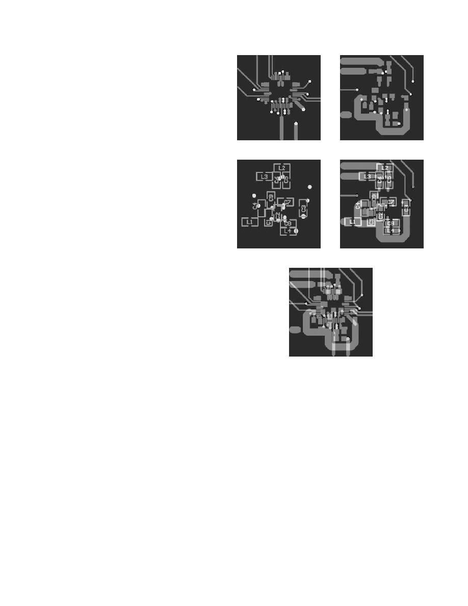
Board Layout and Grounding
To obtain optimum performance from the AD7485, it is recom-
mended that a printed circuit board with a minimum of three
layers is used. One of these layers, preferably the middle layer,
should be as complete a ground plane as possible to give the
best shielding. The board should be designed in such a way that
the analog and digital circuitry are separated and confined to
certain areas of the board. This practice, along with avoiding
running digital and analog lines close together, should help to
avoid coupling digital noise onto analog lines.
The power supply lines to the AD7485 should be approximately
3 mm wide to provide a low impedance path and reduce the
effects of glitches on the power supply lines. It is vital that good
decoupling is also present. A combination of ferrites and
decoupling capacitors should be used as shown in Figure 11.
The decoupling capacitors should be as close to the supply pins
as possible. This is made easier by the use of multilayer boards.
The signal traces from the AD7485 pins can be run on the top
layer while the decoupling capacitors and ferrites mounted on
the bottom layer where the power traces exist. The ground
plane between the top and bottom planes provides excellent
shielding.
Figures 12a–12e show a sample layout of the board area imme-
diately surrounding the AD7485. Pin 1 is the bottom left corner
of the device. Figure 12a shows the top layer where the AD7485
is mounted with vias to the bottom routing layer highlighted.
Figure 12b shows the bottom layer where the power routing is
with the same vias highlighted. Figure 12c shows the bottom
layer silkscreen where the decoupling components are soldered
directly beneath the device. Figure 12d shows the silkscreen
overlaid on the solder pads for the decoupling components, and
Figure 12e shows the top and bottom routing layers overlaid.
The black area in each figure indicates the ground plane present
on the middle layer.
Figure 12a
Figure 12b
Figure 12c
Figure 12d
Figure 12e
C1-6 : 100 nF, C7–8: 470 nF, C9: 1 nF
L1-4: Meggit-Sigma Chip Ferrite Beads (BMB2A0600RS2)
A
相關(guān)PDF資料 |
PDF描述 |
|---|---|
| AD7490BRU-REEL | IC ADC 12BIT 16CH 28-TSSOP T/R |
| AD7492ARZ-5 | IC ADC 12BIT REF/CLOCK 24SOIC |
| AD7495BRM | IC ADC 12BIT SRL LP W/REF 8MSOP |
| AD75004KP | IC DAC 12BIT QUAD W/BUFF 28-PLCC |
| AD7521LN | CONV D/A 12BIT 1MHZ 2LSB 18-DIP |
相關(guān)代理商/技術(shù)參數(shù) |
參數(shù)描述 |
|---|---|
| AD7490 | 制造商:AD 制造商全稱:Analog Devices 功能描述:16-Channel, 1 MSPS, 12-Bit ADC with Sequencer in 28-Lead TSSOP |
| AD7490_12 | 制造商:AD 制造商全稱:Analog Devices 功能描述:16-Channel, 1 MSPS, 12-Bit ADC with Sequencer in 28-Lead TSSOP |
| AD7490BCP | 制造商:Analog Devices 功能描述:ADC Single SAR 1Msps 12-bit Serial 32-Pin LFCSP EP 制造商:Rochester Electronics LLC 功能描述:12 BIT 16 CHANNEL ADC IC - Bulk 制造商:Analog Devices 功能描述:IC 12-BIT ADC |
| AD7490BCP-REEL | 制造商:Analog Devices 功能描述:ADC Single SAR 1Msps 12-bit Serial 32-Pin LFCSP EP T/R |
| AD7490BCP-REEL7 | 制造商:Analog Devices 功能描述:ADC Single SAR 1Msps 12-bit Serial 32-Pin LFCSP EP T/R |
發(fā)布緊急采購,3分鐘左右您將得到回復(fù)。