- 您現(xiàn)在的位置:買賣IC網(wǎng) > PDF目錄375230 > AD1892JR (ANALOG DEVICES INC) Integrated Digital Receiver/Rate Converter PDF資料下載
參數(shù)資料
| 型號(hào): | AD1892JR |
| 廠商: | ANALOG DEVICES INC |
| 元件分類: | 消費(fèi)家電 |
| 英文描述: | Integrated Digital Receiver/Rate Converter |
| 中文描述: | SPECIALTY CONSUMER CIRCUIT, PDSO28 |
| 封裝: | SOIC-28 |
| 文件頁(yè)數(shù): | 13/24頁(yè) |
| 文件大小: | 231K |
| 代理商: | AD1892JR |
第1頁(yè)第2頁(yè)第3頁(yè)第4頁(yè)第5頁(yè)第6頁(yè)第7頁(yè)第8頁(yè)第9頁(yè)第10頁(yè)第11頁(yè)第12頁(yè)當(dāng)前第13頁(yè)第14頁(yè)第15頁(yè)第16頁(yè)第17頁(yè)第18頁(yè)第19頁(yè)第20頁(yè)第21頁(yè)第22頁(yè)第23頁(yè)第24頁(yè)
AD1892
REV. 0
–13–
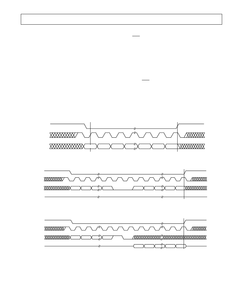
SERIAL CONTROL PORT
The serial control port on the AD1892 is a bidirectional inter-
face that allows external microcontrollers and microprocessors
to gain access to the two on-chip byte-wide control registers and
to the sixteen on-chip byte-wide status registers. The serial
control port is signal compatible with the Serial Peripheral In-
terface (SPI) standard, which has been popularized by Motorola’s
family of microcontroller and microprocessor products.
The basic timing for the serial control port is shown in Figure
17. The CS signal is both a chip select and a latch enable. CS
must be LO for the duration of the read or write cycle. The
CCLK signal is the data clock signal for the serial control port.
The frequency of the CCLK signal must not exceed 1/8 the
frequency of the MCLK signal applied to the AD1892. The
incoming address and write data must be valid on the rising
edge of CCLK, and the outgoing read data is guaranteed to be
valid on the ring edge of CCLK. The SDI signal carries the
serial address and write data to the AD1892. The SDO signal
carries the serial read data from the AD1892. The address and
data information is MSB first.
MSB–1
MSB–2
LSB+2
LSB+1
LSB
CS
CCLK
SDI/SDO
MSB
Figure 17. Serial Control Port Basic Timing
LSB
D0
MSB
D7
DATA
D6
D1
HIGH Z
ADDRESS
MSB
ADDR5
LSB
ADDR0
RES
R/
W
ADDR4
CS
CCLK
SDI
SDO
Figure 18. Serial Control Port Write Cycle
DATA
LSB
MSB
D7
HIGH Z
ADDRESS
MSB
ADDR5
LSB
ADDR0
RES
R/
W
ADDR4
CS
CCLK
SDI
SDO
D6
D1
D0
Figure 19. Serial Control Port Read Cycle
The serial control port write cycle is shown in Figure 18. In the
first byte, the AD1892 defines a six bit write address field, a
read/
write
bit (reset LO for a write cycle) and a reserved (res)
bit. [The reserve (res) bit should be reset LO for both write
and read cycles.] The data byte intended to be written to the
specified write address follows immediately thereafter, MSB
first. All information is carried on the SDI input, with the SDO
output remaining in a high impedance (three-state) condition.
The AD1892 defines only two valid write addresses, Control
Register 1 and Control Register 2, which are defined below.
The serial control port read cycle is shown in Figure 19. The
address information is presented on the SDI input (6-bit ad-
dress, read/
write
set HI and a reserved bit). The data byte output
from the addressed location is transmitted on the SDO output,
MSB first. The AD1892 defines sixteen valid read addresses,
comprising Status Register 1, Status Register 2, four bytes of
Channel Status information and ten bytes of Q-Channel subcode
information. All of these read addresses are defined below.
相關(guān)PDF資料 |
PDF描述 |
|---|---|
| AD1892JRRL | Integrated Digital Receiver/Rate Converter |
| AD1892 | Integrated Digital Receiver/Rate Converter(數(shù)字音頻接收器/采樣率轉(zhuǎn)換器) |
| AD1893JN | Low Cost SamplePort 16-Bit Stereo Asynchronous Sample Rate Converter |
| AD1893JST | Low Cost SamplePort 16-Bit Stereo Asynchronous Sample Rate Converter |
| AD1893 | Low Cost SamplePort 16-Bit Stereo Asynchronous Sample Rate Converter(低成本采樣端口16位立體聲異步采樣率轉(zhuǎn)換器) |
相關(guān)代理商/技術(shù)參數(shù) |
參數(shù)描述 |
|---|---|
| AD1892JRRL | 制造商:Analog Devices 功能描述:Receiver/Rate Converter 28-Pin SOIC W T/R 制造商:Rochester Electronics LLC 功能描述:INTEGRATED DIG.RECEIVER/RATE CONVERTER - Bulk |
| AD1892JRZ | 制造商:Analog Devices 功能描述:Receiver/Rate Converter 28-Pin SOIC W |
| AD1893 | 制造商:AD 制造商全稱:Analog Devices 功能描述:Low Cost SamplePort 16-Bit Stereo Asynchronous Sample Rate Converter |
| AD1893JN | 制造商:Analog Devices 功能描述:Sample Rate Converter 28-Pin PDIP W 制造商:Rochester Electronics LLC 功能描述:LOW COST ASRC PDIP 28-PIN - Bulk |
| AD1893JNZ | 制造商:Analog Devices 功能描述:Sample Rate Converter 28-Pin PDIP W |
發(fā)布緊急采購(gòu),3分鐘左右您將得到回復(fù)。