- 您現(xiàn)在的位置:買賣IC網(wǎng) > PDF目錄375230 > AD10265AZ (ANALOG DEVICES INC) LJT 10C 10#20 SKT RECP PDF資料下載
參數(shù)資料
| 型號: | AD10265AZ |
| 廠商: | ANALOG DEVICES INC |
| 元件分類: | ADC |
| 英文描述: | LJT 10C 10#20 SKT RECP |
| 中文描述: | DUAL 3-CH 12-BIT PROPRIETARY METHOD ADC, PARALLEL ACCESS, CQFP68 |
| 封裝: | CERAMIC, LCC-68 |
| 文件頁數(shù): | 10/18頁 |
| 文件大小: | 267K |
| 代理商: | AD10265AZ |
AD10265
–10–
REV. 0
THEORY OF OPERATION
Refer to the Functional Block Diagram. The AD10265 em-
ploys three monolithic ADI components per channel (AD9631
AD9632 and AD6640), along with multiple passive resistor
networks and decoupling capacitors to fully integrate a com-
plete 12-bit analog-to-digital converter.
The input signal is first passed through a precision laser-trimmed
resistor divider, allowing the user to externally select operation
with a full-scale signal of
±
0.5 V,
±
1.0 V, or
±
2.0 V by choosing
the proper input terminal for the application.
Since the AD6640 implements a true differential analog input,
the AD9631/AD9632 have been configured to provide a differ-
ential input for the AD6640 ADC through ac-coupling. The ac
signal gain of the AD9631/AD9632 can be trimmed to provide a
constant differential input to the AD6640. This allows the con-
verter to be used in multiple system applications without the
need for external gain circuit normally requiring trim. The
AD9631/AD9632 were chosen for their superior ac performance
and input drive capabilities, which have limited the ability of
many amplifiers to drive high performance ADCs. As new am-
plifiers are developed, pin-compatible improvements are planned
to incorporate the latest operational amplifier technology.
APPLYING THE AD10265
Encoding the AD10265
Best performance is obtained by driving the encode pins differ-
entially. However, the AD10265 is also designed to interface
with TTL and CMOS logic families. The source used to drive
the ENCODE pin(s) must be clean and free from jitter. Sources
with excessive jitter will limit SNR and overall performance.
0.01
m
F
TTL OR CMOS
SOURCE
ENCODE
ENCODE
AD10265
Figure 14. Single-Ended TTL/CMOS Encode
The AD10265 encode inputs are connected to a differential
input stage (see Figure 4 under Equivalent Circuits). With no
input connected to either ENCODE pin, the voltage divider
biases the inputs to 1.6 volts. For TTL or CMOS usage, the
encode source should be connected to ENCODE.
ENCODE
should be decoupled using a low inductance or microwave chip
capacitor to ground.
If a logic threshold other than the nominal +1.6 V is required,
the following equations show how to use an external resistor,
Rx, to raise or lower the trip point (see Figure 4, R1 = 17 k
,
R2 = 8 k
).
V
R Rx
1
1 2
R Rx
2
1
5R R
+
=
+
x
to lower logic threshold.
0.01
m
F
ENCODE
SOURCE
ENCODE
ENCODE
AD10265
R
x
V
1
+5V
R1
R2
Figure 15. Lower Threshold for Encode
V
R
R Rx
R
1
+
R
Rx
1
5 2
2
1
=
+
to raise logic threshold.
0.01
m
F
ENCODE
SOURCE
ENCODE
ENCODE
AD10265
R
x
V
1
+5V
R1
R2
AV
CC
Figure 16. Raise Logic Threshold for Encode
While the single-ended encode will work well for many applica-
tions, driving the encode differentially will provide increased
performance. Depending on circuit layout and system noise, a
1 dB to 3 dB improvement in SNR can be realized. It is recom-
mended that differential TTL logic be used, however, because
most TTL families that support complementary outputs are not
delay or slew rate matched. Instead, it is recommended that the
encode signal be ac-coupled into the ENCODE and
ENCODE
pins.
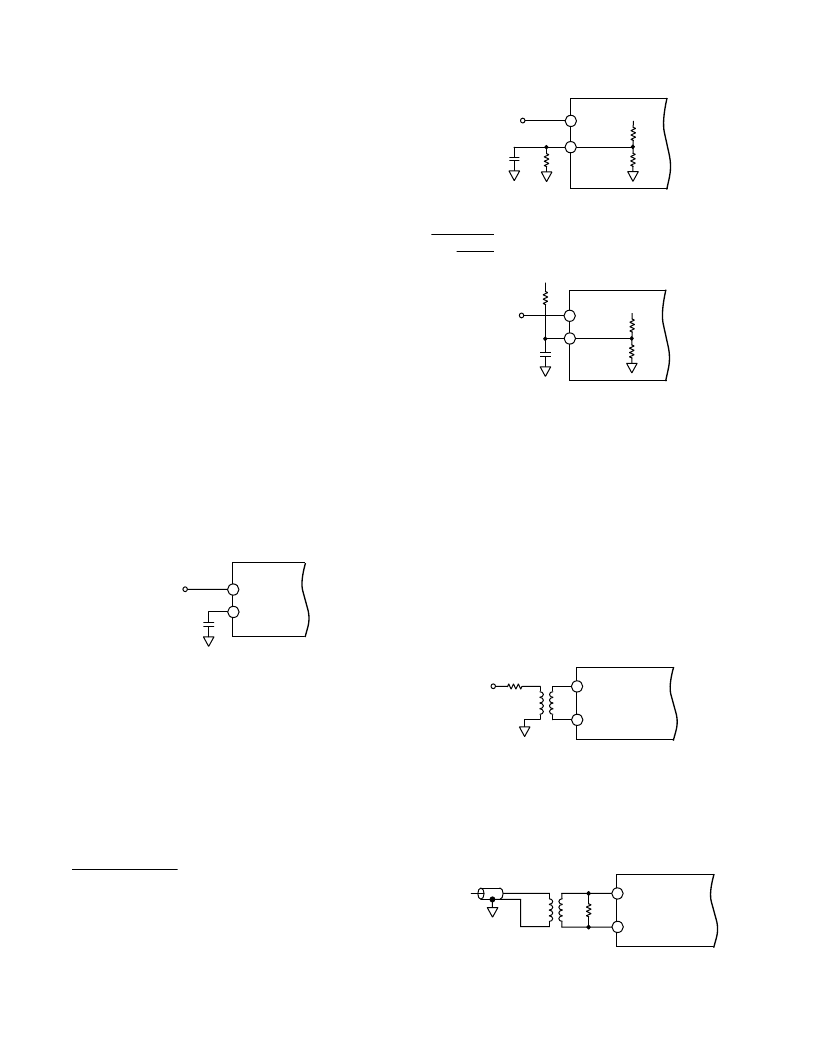
The simplest option is shown below. The low jitter TTL signal
is coupled with a limiting resistor, typically 100
, to the pri-
mary side of an RF transformer (these transformers are inexpen-
sive and readily available; part number in Figure 17 is from Mini-
Circuits). The secondary side is connected to the ENCODE
and
ENCODE
pins of the converter. Since both encode inputs
are self-biased, no additional components are required.
TTL
ENCODE
ENCODE
AD10265
100
V
T1–1T
Figure 17. TTL Source—Differential Encode
A clean sine wave may be substituted for a TTL clock. In this
case, the matching network is shown below. Select a transformer
ratio to match source and load impedances. The input imped-
ance of the AD10265 encode is approximately 11 k
differen-
tially. Therefore “R,” shown in Figure 18, may be any value that
is convenient for available drive power.
ENCODE
ENCODE
AD10265
R
T1–1T
SINE
SOURCE
Figure 18. Sine Source—Differential Encode
相關(guān)PDF資料 |
PDF描述 |
|---|---|
| AD10677 | 16-Bit, 65 MSPS A/D Converter |
| AD10677BWS | 16-Bit, 65 MSPS A/D Converter |
| AD120 | 3-Level / 258 Outputs TFT LCD Gate Driver |
| AD120T | 3-Level / 258 Outputs TFT LCD Gate Driver |
| AD1380JD | Low Cost 16-Bit Sampling ADC |
相關(guān)代理商/技術(shù)參數(shù) |
參數(shù)描述 |
|---|---|
| AD10265PCB | 制造商:AD 功能描述:10265 ANALOG DEVICE S8M6A |
| AD102JY | 制造商:Analog Devices 功能描述:IC AMP ISOLATION 102J DIP9 |
| AD103 | 制造商:Microsemi Corporation 功能描述:THYRISTOR SCR 300V 15A 3PIN TO-39 - Bulk |
| AD-103 | 制造商:B&K Precision Corporation 功能描述: |
| AD1036-12FS | 制造商:MPD 制造商全稱:MicroPower Direct, LLC 功能描述:Very Low Cost, 36 - 48W DIN Rail Mount Single Output AC/DC Power Supplies |
發(fā)布緊急采購,3分鐘左右您將得到回復(fù)。