- 您現(xiàn)在的位置:買賣IC網(wǎng) > PDF目錄36338 > 935261617112 (NXP SEMICONDUCTORS) SERIAL INPUT LOADING, 24-BIT DAC, PDSO32 PDF資料下載
參數(shù)資料
| 型號: | 935261617112 |
| 廠商: | NXP SEMICONDUCTORS |
| 元件分類: | DAC |
| 英文描述: | SERIAL INPUT LOADING, 24-BIT DAC, PDSO32 |
| 封裝: | 7.50 MM, PLASTIC, SO-32 |
| 文件頁數(shù): | 3/31頁 |
| 文件大小: | 199K |
| 代理商: | 935261617112 |
第1頁第2頁當(dāng)前第3頁第4頁第5頁第6頁第7頁第8頁第9頁第10頁第11頁第12頁第13頁第14頁第15頁第16頁第17頁第18頁第19頁第20頁第21頁第22頁第23頁第24頁第25頁第26頁第27頁第28頁第29頁第30頁第31頁
2000 Jan 04
11
Philips Semiconductors
Preliminary specication
Multi-channel lter DAC
UDA1328T
9
L3 INTERFACE DESCRIPTION
The following system and digital sound processing
features can be controlled in the microcontroller mode of
the UDA1328:
Data input format
De-emphasis for 32, 44.1, 48 and 96 kHz
Volume control: master and for individual channels
Soft or quick mute: master and for individual channels
Output polarity control: master and for individual
channels
Digital silence control: master and for individual
channels
Power-down mode.
The exchange of data and control information between the
microcontroller and the UDA1328 is accomplished via a
serial hardware interface comprising the following pins:
L3DATA: microcontroller interface data line
L3MODE: microcontroller interface mode line
L3CLOCK: microcontroller interface clock line.
Information transfer via the microcontroller bus is
organized LSB first and is in accordance with the so called
‘L3’ format, in which two different modes of operation can
be distinguished. The address mode and data transfer
mode are illustrated in Figs 6 and 7.
The address mode is required to select a device
communicating via the L3-bus and to define the
destination registers for the data transfer mode. Data
transfer for the UDA1328 can only be in one direction;
input to the UDA1328 to program its sound processing and
other functional features.
9.1
Address mode
The address mode is used to select a device for
subsequent data transfer and to define the destination
registers. The address mode is characterized by L3MODE
being LOW and a burst of 8 pulses on L3CLOCK,
accompanied by 8 data bits. The fundamental timing is
shown in Fig.6. Data bits 0 and 1 indicate the type of
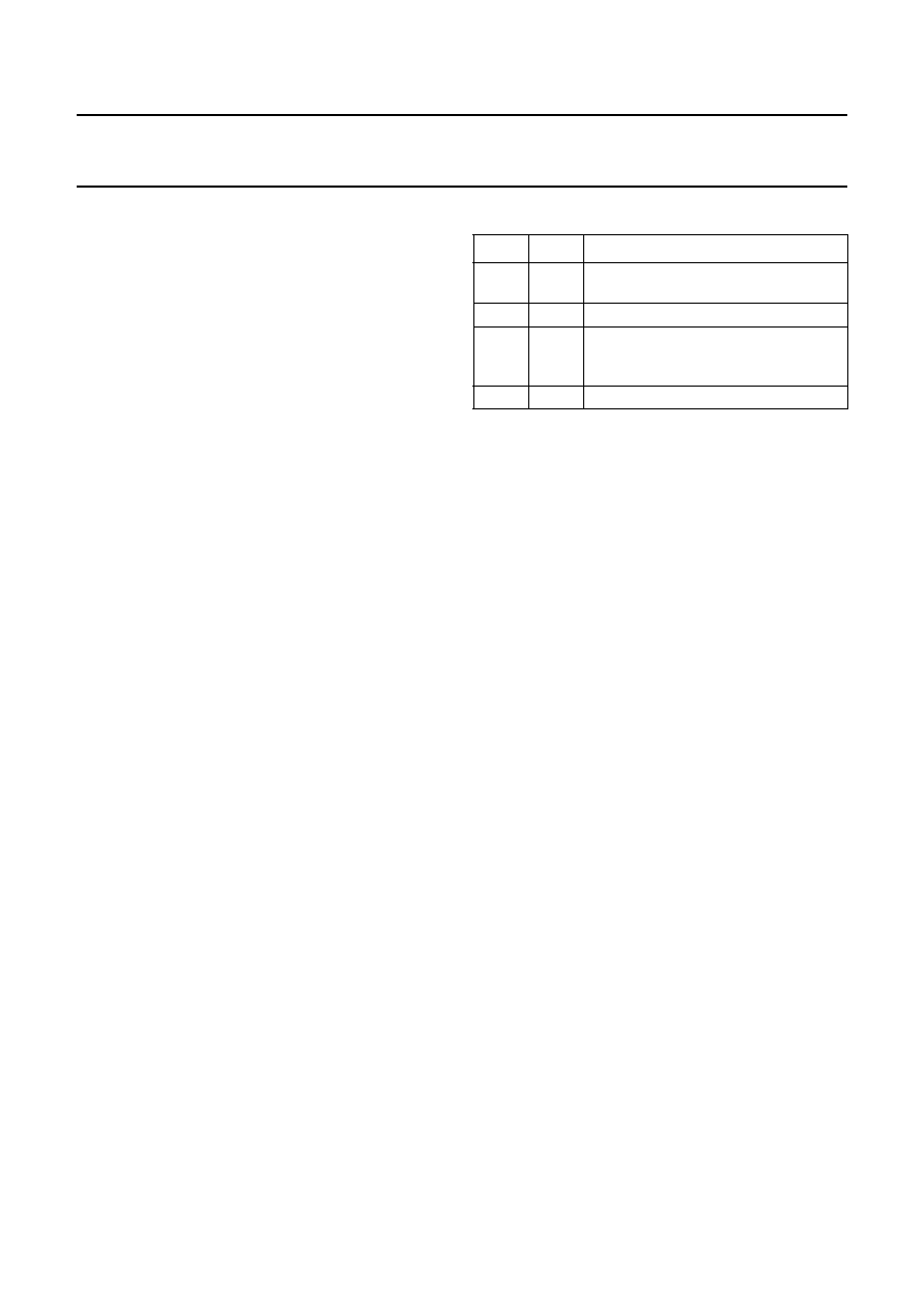
subsequent data transfer as given in Table 5.
Table 5
Selection of data transfer
Data bits 7 to 2 represent a 6-bit device address, with bit 7
being the MSB and bit 2 the LSB. The address of the
UDA1328 is 000100 (bit 7 to bit 2) when L3ADR
(DEEM0) = LOW or 000101 when L3ADR = HIGH. In the
event that the UDA1328 receives a different address, it will
deselect its microcontroller interface logic.
9.2
Data transfer mode
The selection preformed in the address mode remains
active during subsequent data transfers, until the
UDA1328 receives a new address command. The
fundamental timing of data transfers is essentially the
same as in the address mode, shown in Fig.6. The
maximum input clock and data rate is 64fs. All transfers are
byte wise, i.e. they are based on groups of 8 bits. Data will
be stored in the UDA1328 after the eighth bit of a byte has
been received. A multibyte transfer is illustrated in Fig.8.
9.2.1
PROGRAMMING THE SOUND PROCESSING AND
OTHER FEATURES
The sound processing and other feature values are stored
in independent registers. The first selection of the registers
is achieved by the choice of data type that is transferred.
This is performed in the address mode, bit 1 and bit 0
(see Table 5). The second selection is performed by the
2 MSBs of the data byte (bit 7 and bit 6). The other bits in
the data byte (bit 5 to bit 0) is the value that is placed in the
selected registers.
When the data transfer of type ‘data’ is selected, the
features volume, sub volume, de-emphasis, mute, digital
silence settings, output polarity control and channel
selection can be controlled. When the data transfer of type
‘status’ is selected, the features system clock frequency,
data input format, mute mode and power control can be
controlled.
BIT 1
BIT 0
TRANSFER
0
data (volume, de-emphasis, mute,
digital silence mode, polarity control)
0
1
not used
1
0
status (system clock frequency,
data input format, mute mode,
power control)
1
not used
相關(guān)PDF資料 |
PDF描述 |
|---|---|
| 935261695118 | 0.25 A SWITCHING REGULATOR, 50 kHz SWITCHING FREQ-MAX, PDSO8 |
| 935256880112 | 0.25 A SWITCHING REGULATOR, 50 kHz SWITCHING FREQ-MAX, PDIP8 |
| 935261695112 | 0.25 A SWITCHING REGULATOR, 50 kHz SWITCHING FREQ-MAX, PDSO8 |
| 935261770518 | 1-CH 9-BIT PROPRIETARY METHOD ADC, PARALLEL ACCESS, PDSO28 |
| 935261770112 | 1-CH 9-BIT PROPRIETARY METHOD ADC, PARALLEL ACCESS, PDSO28 |
相關(guān)代理商/技術(shù)參數(shù) |
參數(shù)描述 |
|---|---|
| 935262025112 | 制造商:NXP Semiconductors 功能描述:SUB ONLY IC |
| 935262217118 | 制造商:NXP Semiconductors 功能描述:Real Time Clock Serial 8-Pin SO T/R |
| 935264217557 | 制造商:NXP Semiconductors 功能描述:SUB ONLY IC |
| 935267356112 | 制造商:NXP Semiconductors 功能描述:IC TEA1507PN |
| 935268081112 | 制造商:NXP Semiconductors 功能描述:SUB ONLY IC |
發(fā)布緊急采購,3分鐘左右您將得到回復(fù)。