- 您現(xiàn)在的位置:買賣IC網(wǎng) > PDF目錄36337 > 935261504557 (NXP SEMICONDUCTORS) SPECIALTY CONSUMER CIRCUIT, PQFP44 PDF資料下載
參數(shù)資料
| 型號(hào): | 935261504557 |
| 廠商: | NXP SEMICONDUCTORS |
| 元件分類: | 消費(fèi)家電 |
| 英文描述: | SPECIALTY CONSUMER CIRCUIT, PQFP44 |
| 封裝: | PLASTIC, SOT-307, QFP-44 |
| 文件頁(yè)數(shù): | 15/87頁(yè) |
| 文件大小: | 440K |
| 代理商: | 935261504557 |
第1頁(yè)第2頁(yè)第3頁(yè)第4頁(yè)第5頁(yè)第6頁(yè)第7頁(yè)第8頁(yè)第9頁(yè)第10頁(yè)第11頁(yè)第12頁(yè)第13頁(yè)第14頁(yè)當(dāng)前第15頁(yè)第16頁(yè)第17頁(yè)第18頁(yè)第19頁(yè)第20頁(yè)第21頁(yè)第22頁(yè)第23頁(yè)第24頁(yè)第25頁(yè)第26頁(yè)第27頁(yè)第28頁(yè)第29頁(yè)第30頁(yè)第31頁(yè)第32頁(yè)第33頁(yè)第34頁(yè)第35頁(yè)第36頁(yè)第37頁(yè)第38頁(yè)第39頁(yè)第40頁(yè)第41頁(yè)第42頁(yè)第43頁(yè)第44頁(yè)第45頁(yè)第46頁(yè)第47頁(yè)第48頁(yè)第49頁(yè)第50頁(yè)第51頁(yè)第52頁(yè)第53頁(yè)第54頁(yè)第55頁(yè)第56頁(yè)第57頁(yè)第58頁(yè)第59頁(yè)第60頁(yè)第61頁(yè)第62頁(yè)第63頁(yè)第64頁(yè)第65頁(yè)第66頁(yè)第67頁(yè)第68頁(yè)第69頁(yè)第70頁(yè)第71頁(yè)第72頁(yè)第73頁(yè)第74頁(yè)第75頁(yè)第76頁(yè)第77頁(yè)第78頁(yè)第79頁(yè)第80頁(yè)第81頁(yè)第82頁(yè)第83頁(yè)第84頁(yè)第85頁(yè)第86頁(yè)第87頁(yè)
1999 Jul 01
22
Philips Semiconductors
Product specication
9-bit video input processor
SAA7113H
8.5
Synchronization
The prefiltered luminance signal is fed to the
synchronization stage. Its bandwidth is further reduced to
1 MHz in a low-pass filter. The sync pulses are sliced and
fed to the phase detectors where they are compared with
the sub-divided clock frequency. The resulting output
signal is applied to the loop filter to accumulate all phase
deviations. Internal signals (e.g. HCL and HSY) are
generated in accordance with analog front-end
requirements. The loop filter signal drives an oscillator to
generate the line frequency control signal LFCO,
see Fig.19.
The detection of ‘pseudo syncs’ as part of the macrovision
copy protection standard is also done within the
synchronization circuit.
The result is reported as flag COPRO within the decoder
status byte at subaddress 1FH.
8.6
Clock generation circuit
The internal CGC generates all clock signals required for
the video input processor. The internal signal LFCO is a
digital-to-analog converted signal provided by the
horizontal PLL. It is the multiple of the line frequency
[6.75 MHz = 429
× fH (50 Hz) or 432 × fH (60 Hz)].
Internally the LFCO signal is multiplied by a factor of
2 and 4 in the PLL circuit (including phase detector, loop
filtering, VCO and frequency divider) to obtain the output
clock signals. The rectangular output clocks have a 50%
duty factor.
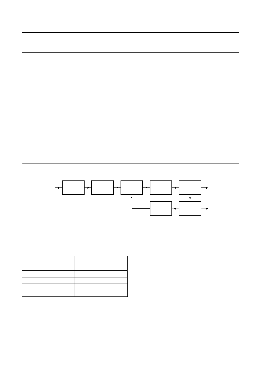
Fig.20 Block diagram of clock generation circuit.
handbook, full pagewidth
BAND PASS
FC = LLC/4
ZERO
CROSS
DETECTION
PHASE
DETECTION
LOOP
FILTER
DIVIDER
1/2
DIVIDER
1/2
OSCILLATOR
MHB330
LLC2
LLC
LFCO
Table 1
Clock frequencies
CLOCK
FREQUENCY (MHz)
XTAL
24.576
LLC
27
LLC2 (internal)
13.5
LLC4 (internal)
6.75
LLC8 (virtual)
3.375
8.7
Power-on reset and CE input
A missing clock, insufficient digital or analog VDDA0 supply
voltages (below 2.8 V) will initiate the reset sequence; all
outputs are forced to 3-state (see Fig.21).
It is possible to force a reset by pulling the Chip Enable
(CE) to ground. After the rising edge of CE and sufficient
power supply voltage, the outputs LLC and SDA return
from 3-state to active, while RTS0, RTS1 and RTCO
remain in 3-state and have to be activated via I2C-bus
programming (see Table 2).
相關(guān)PDF資料 |
PDF描述 |
|---|---|
| 935261537118 | DELTA-SIGMA ADC, PDSO16 |
| 935261537112 | DELTA-SIGMA ADC, PDSO16 |
| 935261615112 | SPECIALTY CONSUMER CIRCUIT, PDSO28 |
| 935261615118 | SPECIALTY CONSUMER CIRCUIT, PDSO28 |
| 935261616112 | SPECIALTY CONSUMER CIRCUIT, PDIP32 |
相關(guān)代理商/技術(shù)參數(shù) |
參數(shù)描述 |
|---|---|
| 935262025112 | 制造商:NXP Semiconductors 功能描述:SUB ONLY IC |
| 935262217118 | 制造商:NXP Semiconductors 功能描述:Real Time Clock Serial 8-Pin SO T/R |
| 935264217557 | 制造商:NXP Semiconductors 功能描述:SUB ONLY IC |
| 935267356112 | 制造商:NXP Semiconductors 功能描述:IC TEA1507PN |
| 935268081112 | 制造商:NXP Semiconductors 功能描述:SUB ONLY IC |
發(fā)布緊急采購(gòu),3分鐘左右您將得到回復(fù)。